Enjoy complimentary customisation on priority with our Enterprise License!
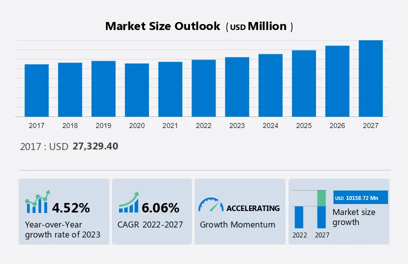
The semiconductor packaging materials market size is estimated to grow by USD 10.15 billion at a CAGR of 6.06% between 2022 and 2027.
The market's expansion hinges on several factors, notably the rising trend of miniaturizing electronic devices and the burgeoning use of semiconductor integrated circuits (ICs) in IoT applications. Advanced semiconductor material packaging technologies further drive growth alongside the increasing global demand for consumer electronics and smart devices. This surge reflects a growing appetite for innovative electronic solutions across various industries. The convergence of these factors underscores a promising trajectory for semiconductor ICs, positioning them as pivotal components in powering the next generation of interconnected and intelligent electronic devices.
To learn more about this report, View Report Sample
The market continues to thrive with the growing demand for electronic equipment and the advancement of semiconductor integration technologies. Innovations like 3D semiconductor packaging technology and fan-out wafer-level packaging are reshaping the landscape, supported by a robust ecosystem of semiconductor packaging suppliers. Interposers and bridges play a vital role in enhancing energy efficiency and optimizing process nodes in semiconductor manufacturing. The AP (advanced packaging) industry is witnessing significant growth, driven by increasing computing power and the proliferation of artificial intelligence applications. This growth extends to various sectors, including IoT devices, automotive electronics, data center equipment, and the rapid deployment of 5G technology. Consumer electronics, smartphones, and IoT devices rely on efficient semiconductor packaging solutions to deliver high-speed connectivity, with chips, wires, and signals powering the backbone of 5G infrastructure, transitioning from 4G to the next generation of connectivity.
These packaging solutions are crucial for various applications, from PC/laptops to vehicle electrification, aiming to reduce emissions and enhance efficiency. In smart corporate settings, wireless broadband (WiBro) technology is revolutionizing connectivity, while semiconductor packaging companies are leveraging ultra-high-density fan-out (UHD FO) techniques to optimize inputs and outputs (I/O). With a focus on miniaturization and performance, square millimeter and line and spacing (L/S) measurements are key considerations, along with features like redistribution layers (RDL) in the upgraded versions of semiconductor packaging units. These innovations underscore the Semiconductor Industry Association's efforts to drive advancements in the industry. Our researchers analyzed the data with 2022 as the base year, along with the key drivers, trends, and challenges. A holistic analysis of drivers will help companies refine their marketing strategies to gain a competitive advantage.
One of the key factors driving the market growth is the rise in global demand for smart electronic devices. Due to the rise in the demand for semiconductor equipment electronics and smart electronic devices, the global consumer electronics market is expected to grow at a CAGR of more than 12% during the forecast period. Factors such as the rise in the sales of smart devices such as smartwatches, smartphones, and smart bands globally are fuelling the demand for ICs integrated together for manufacturing these devices.
As a result, it has fuelled the growth of semiconductor materials. Some of the key applications of IC and semiconductors include Tablets and smartphones. Other applications of semiconductors include Wi-Fi connectivity, multimedia streaming, touchscreens, and access to the Internet are based on the signals that are generated within high-tech circuits within the device which are embedded with semiconductor chips. Hence, such applications are expected to drive the market growth during the forecast period.
A key factor shaping the market growth is the increase in the adoption of semiconductor ICs for automobiles and the shift toward copper as bonding wire material. There is a rising need for semiconductor wafers due to the automation and electrification of automobiles. Some of the key applications of semiconductor ICs that are used in automotive products are anti-lock braking systems, car navigation, airbag control, GPS, and display, power doors and windows, collision detection technology, infotainment, and automated driving.
As a result, the rise in car production will drive the demand for semiconductor chips which in turn will fuel the demand devices, associated packaging materials, and assembly equipment market. Factors such as the rise in the adoption of semiconductor ICs for automobiles and the transition toward copper as bonding wire material are some of the trends, which is expected to fuel the growth of the global market trends during the forecast period.
Regulations associated with semiconductor packaging materials are one of the key challenges hindering market growth. One of the key challenges for semiconductor Companies is complying with strict material specifications set down by packaging assemblers and testers. As there is a growing concern for environmental hazards related to packaging, semiconductor chemical and materials suppliers are facing increased environmental regulations, especially in developing countries.
For instance, the restriction of hazardous substances (RoHS) directive calls for the removal of metals such as polybrominated biphenyls (PBB), mercury, bismuth, chromium VI, lead, and cadmium, as well as ozone-depleting substances from all PCB and semiconductor packaging materials. With the exception of exempt applications, the implementation of RoHS is well underway, and most global suppliers have already developed 'green' alternatives. Hence, such factors are expected to significantly hinder the market during the forecast period.
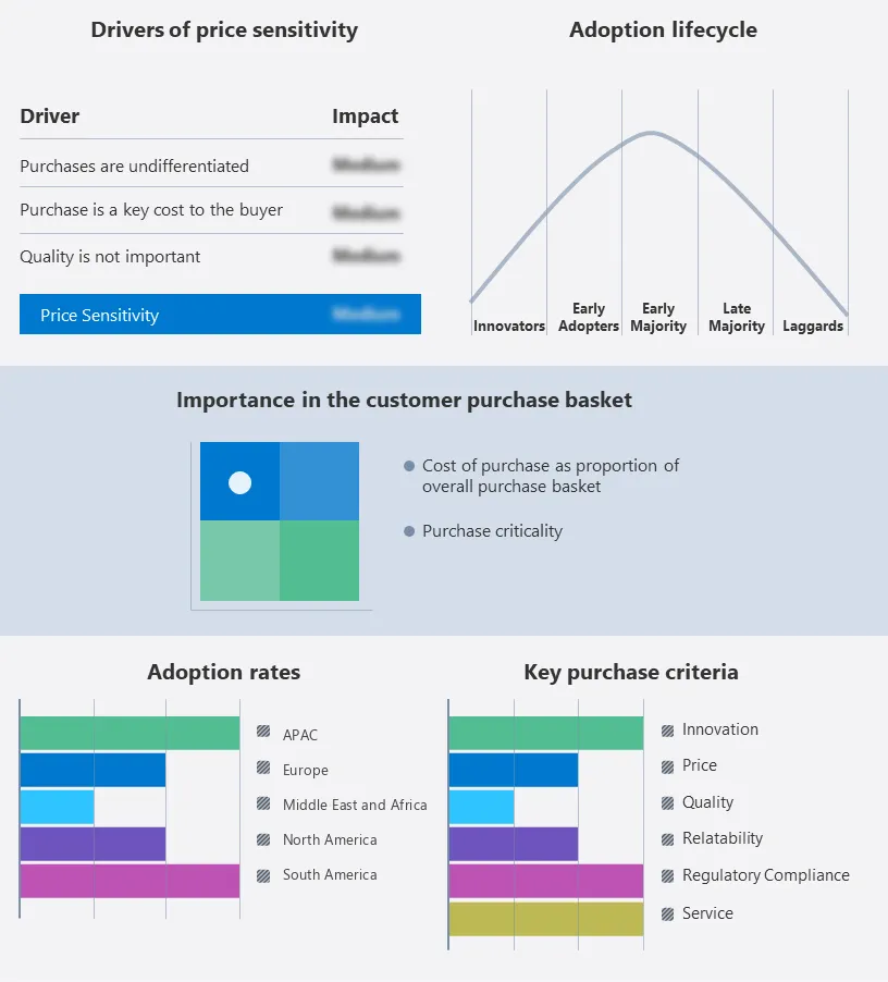
The market research and growth report includes the adoption lifecycle of the market, covering from the innovator’s stage to the laggard’s stage. It focuses on adoption rates in different regions based on penetration. Furthermore, the market growth and forecasting report also includes key purchase criteria and drivers of price sensitivity to help companies evaluate and develop their growth strategies.
Customer Landscape
Companies are implementing various strategies, such as strategic alliances, partnerships, mergers and acquisitions, geographical expansion, and product/service launches, to enhance their presence in the market.
Amkor Technology Inc: The company offers semiconductor packaging materials such as copper leadframe substrates.
The market growth analysis report also includes detailed analyses of the competitive landscape of the market and information about 15 market Companies, including:
Qualitative and quantitative analysis of Companies has been conducted to help clients understand the wider business environment as well as the strengths and weaknesses of key market players. Data is qualitatively analyzed to categorize Companies as pure play, category-focused, industry-focused, and diversified; it is quantitatively analyzed to categorize Companies as dominant, leading, strong, tentative, and weak.
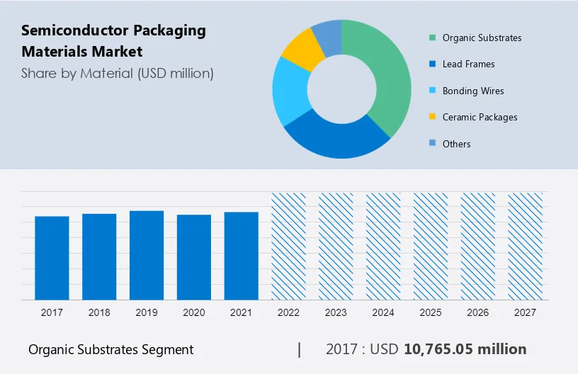
The market share growth by the organic substrates segment will be significant during the forecast period. There is a rising demand for organic substrates in semiconductor packaging as these materials are used these materials are base layers of individual semiconductor devices and ICs on which other layers are deposited to complete the circuit. These materials are a part of the circuit, and it is important that these are efficient conductors of electricity and thinner core materials which are preferably used to surround these in demanding system applications.
Get a glance at the market contribution of various segments View the PDF Sample
The organic substrates segment was valued at USD 10.76 billion in 2017. One of the key reasons for the increasing adoption of organic substrates when compared to lead frames and bonding wires is that the industry advances more toward leadless and cable-less packages. The main advantage of these segments is their flexibility which allows them to be used as interconnects. One of the main Companies which offer organic substrates includes Samsung Electro-Mechanics which offers organic substrates for semiconductor packaging, catering to various industries, such as mobile devices, automotive, and Internet of Things (IoT) applications. Hence, such applications are expected to drive the growth of this segment which, in turn, will drive the market during the forecast period.
For more insights on the market share of various regions Download PDF Sample now!
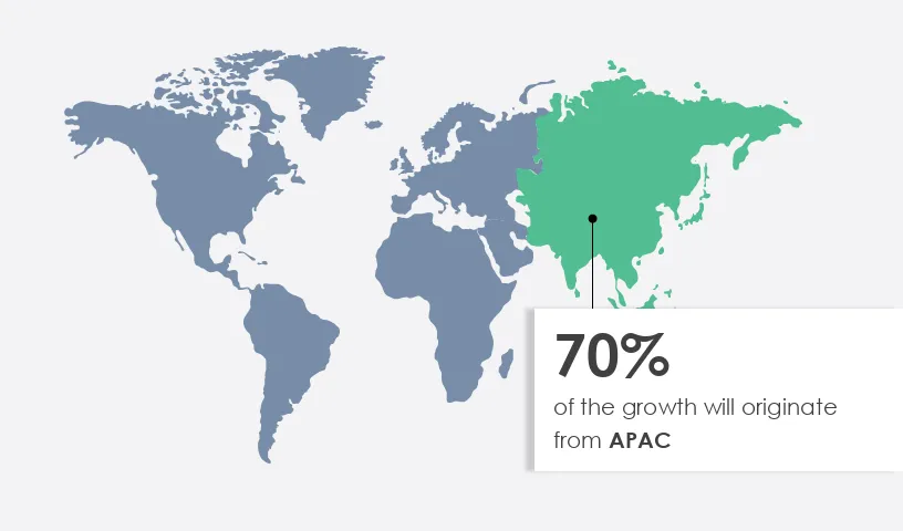
APAC is estimated to contribute 70% to the growth of the global market during the forecast period. Technavio’s analysts have elaborately explained the regional trends and drivers that shape the market during the forecast period. Some of the key regions in APAC that drive the global market growth include countries like Taiwan, China, Japan, and South Korea. These countries house home-bred companies as well as international corporations introducing innovative offerings. The growing adoption of smart mobile devices and consumer electronic goods is driving the growth in the adoption of semiconductor packaging in these countries. Factors such as the availability of cheap labor, raw materials, and favorable factors of production have led to international corporations having scaled up their manufacturing operations in China making it a prominent player in the growth of the market. Hence, such factors are expected to drive the market growth in the region during the forecast period.
The market is propelled by the increasing demand for electronic equipment and the adoption of advanced semiconductor integration techniques. Key trends include the emergence of 3D semiconductor packaging technology and fan-out wafer-level packaging, driven by semiconductor packaging suppliers and die manufacturers. This growth is supported by the semiconductor design sector, which relies on encapsulants, underfill materials, die-attach techniques, and solder balls. Smart homes and corporate settings, along with high-speed internet and wireless broadband, fuel demand, particularly for memory chipmakers and interposers. Innovations in energy-efficient processes and AP (advanced packaging) techniques are reshaping computing power, artificial intelligence, and storage solutions.
The industry is undergoing digital transformation, embracing smart manufacturing practices to enhance semiconductor sales and meet the demand for ultra-high-density packaging solutions. Emerging technologies like Si Interposers and ultra-high-density I/O are driving advancements in heterogeneous dies and low-profile semiconductor packages. As the demand for mission-critical applications and low-latency 5G services grows, the semiconductor sector, including integrated circuits chipset manufacturers, is poised to capitalize on innovations in chip production and semiconductor manufacturing. The ecosystem, spanning the semiconductor value chain from foundry services to flip chip segments, continues to evolve to meet the needs of diverse industries such as IoT devices, automotive electronics, and data center equipment. Key packaging technologies like System-in-Package (SiP), Fan-Out Wafer-Level Packaging (FOWLP), and 3D Integrated Circuits (ICs) are pivotal in enabling advancements in 5G technology and supporting initiatives such as the United States government's CHIPS Act 2022. Materials like ceramics, polymers, solder, conductive adhesives, and wire bonds play a crucial role in ensuring the reliability and performance of semiconductor packages across various applications and industries.
The market forecasting report forecasts market growth by revenue at global, regional & country levels and provides an analysis of the latest trends and growth opportunities from 2017 to 2027.
|
Market Scope |
|
|
Market Report Coverage |
Details |
|
Page number |
206 |
|
Base year |
2022 |
|
Historic period |
2017-2021 |
|
Forecast period |
2023-2027 |
|
Growth momentum & CAGR |
Accelerate at a CAGR of 6.06% |
|
Market growth 2023-2027 |
USD 10.15 billion |
|
Market structure |
Fragmented |
|
YoY growth 2022-2023(%) |
4.52 |
|
Regional analysis |
APAC, North America, Europe, South America, and Middle East and Africa |
|
Performing market contribution |
APAC at 70% |
|
Key countries |
US, China, Taiwan, Japan, and South Korea |
|
Competitive landscape |
Leading Companies, Market Positioning of Companies, Competitive Strategies, and Industry Risks |
|
Key companies profiled |
Amkor Technology Inc., ASE Technology Holding Co. Ltd., BASF SE, ChipMOS TECHNOLOGIES INC., DuPont de Nemours Inc., Henkel AG and Co. KGaA, Heraeus Holding GmbH, Hitachi Ltd., Honeywell International Inc., Indium Corp., Intel Corp., KYOCERA Corp., LG Innotek Co. Ltd., MITSUI and CO. LTD., Nan Ya Printed Circuit Board Corp., Nippon Steel Corp., Powertech Technology Inc., Samsung Electronics Co. Ltd., Taiwan SEMICONDUCTOR CO. LTD, and Texas Instruments Inc. |
|
Market dynamics |
Parent market analysis, Market growth inducers and obstacles, Fast-growing and slow-growing segment analysis, COVID-19 impact and recovery analysis and future consumer dynamics, and Market condition analysis for the forecast period. |
|
Customization purview |
If our report has not included the data that you are looking for, you can reach out to our analysts and get segments customized. |
We can help! Our analysts can customize this market research report to meet your requirements.
1 Executive Summary
2 Market Landscape
3 Market Sizing
4 Historic Market Size
5 Five Forces Analysis
6 Market Segmentation by Material
7 Market Segmentation by End-user
8 Customer Landscape
9 Geographic Landscape
10 Drivers, Challenges, and Trends
11 Vendor Landscape
12 Vendor Analysis
13 Appendix
Get lifetime access to our
Technavio Insights


