
Mask Inspection Equipment Market Size 2024-2028
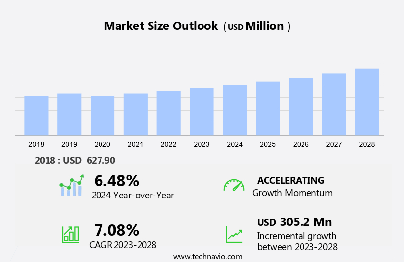
The mask inspection equipment market size is forecast to increase by USD 305.2 million, at a CAGR of 7.08% between 2023 and 2028. Market growth across various sectors hinges on strategic investments in critical infrastructure. Firstly, the semiconductor industry is experiencing growth due to increasing investments in new fabs (fabrication facilities), aimed at expanding production capacity to meet global demand for electronic devices. Secondly, the automotive sector is witnessing significant investments in autonomous vehicles, driven by advancements in artificial intelligence and automotive technology. These investments are fueling innovation and adoption, propelling market expansion. Additionally, there is a surge in investment in data centers to support the growing demand for cloud computing and digital services. This infrastructure investment enhances data processing capabilities, scalability, and reliability, catering to the expanding digital economy. Together, these strategic investments underscore the dynamic interplay between technological advancements and market growth, shaping future opportunities across multiple industries.
What will be the Size of the Market During the Forecast Period?
For More Highlights About this Report, Request Free Sample
Market Dynamic and Customer Landscape
The market is driven by the increasing demand for semiconductor devices in consumer electronics and the semiconductor industry. Photomask inspection plays a crucial role in the manufacture of semiconductor devices, including semiconductor wafers and photomasks, during production. Inspection tools are essential for ensuring the quality of these products and detecting defects. The market for mask inspection equipment is significant due to the high volume of manufacturing in fabrication facilities worldwide. Actinic inspection technology is commonly used for defect inspection, providing high resolution and low noise imaging. Zerodefect masks and absorber pattern inspection are also important applications. Policies and regulations in various nations impact the market, with some nations relying heavily on resource utilization and others addressing the shortage of semiconductors through cutting-edge metrology. The inspection business is a critical component of the semiconductor metrology market, and the demand for these tools continues to grow with the increasing production of semiconductor devices. High volume manufacturing and the need for zero-defect masks have led to the development of advanced inspection tools. These tools are essential for ensuring the quality of semiconductor devices and reducing raw material waste. Die-to-die inspection is another application of mask inspection equipment, which is becoming increasingly important in the semiconductor industry.
Key Market Driver
Growing investment in new fabs is notably driving market growth. Mask inspection equipment plays a crucial role in the semiconductor industry by ensuring the quality of photomasks used in the manufacture of semiconductor devices. Photomasks are essential in the production of semiconductor wafers, which form the basis of various consumer electronics. The semiconductor demand continues to surge, leading to an increased reliance on semiconductor metrology and inspection business in nations with robust semiconductor industries. Photomask inspection tools are indispensable in high-volume manufacturing and fabrication facilities. These tools employ cutting-edge metrology and inspection technologies such as actinic inspection and high-resolution, low-noise imaging.
In addition, they help in the detection of defects like absorber pattern inspection and zerodefect masks, ensuring the production of high-quality semiconductor devices. Semiconductor device manufacturers and mask shops heavily rely on these tools for Die to Die (DB) inspection, ensuring minimal raw material waste and maintaining a backlog of orders. With the ongoing semiconductor demand and potential disruptions due to policies, reliance on semiconductor sourcing from various nations, and the possibility of border closures, the need for efficient and reliable mask inspection equipment is more pressing than ever. Thus, such factors are driving the growth of the market during the forecast period.
Key Market Trends
Increasing demand for portable and handheld mask inspection devices is the key trend in the market. Mask inspection equipment plays a crucial role in the semiconductor industry by ensuring the quality of photomasks used in the manufacture of semiconductor devices. These tools are essential in the production of semiconductor wafers for various consumer electronics and high-volume manufacturing in fabrication facilities. The semiconductor demand and reliance on semiconductors for various industries have led to an increase in the inspection business in nations with favorable policies for semiconductor sourcing. Photomask inspection tools employ advanced technologies like actinic inspection and high resolution, low noise imaging for defect inspection. They are used for absorber pattern inspection, Die to Die comparison (DB), and Zerodefect masks to ensure the highest quality in semiconductor metrology.
Further, the shortage of semiconductors due to disruptions in supply chains and borders has increased the backlog of orders, making efficient resource utilization and cutting-edge metrology more important than ever. Semiconductor Device Manufacturers and Mask Shops rely on these inspection tools to maintain the quality of their products and meet the growing demand for semiconductors. High-performance inspection tools enable the production of defect-free semiconductors, reducing raw material waste and ensuring the timely delivery of products to consumers. Thus, such trends will shape the growth of the market during the forecast period.
Major Market Challenge
Cyclic nature of semiconductor industry is the major challenge that affects the growth of the market. Mask inspection equipment plays a crucial role in the semiconductor industry, ensuring the production of defect-free photomasks for the manufacture of semiconductor devices. These tools are essential for inspecting photomasks used in the production of semiconductor wafers, which are integral to consumer electronics and various industries with increasing semiconductor demand. Advanced inspection technologies, such as actinic inspection, are employed to detect even the slightest defects. Semiconductor metrology companies provide inspection business solutions to various nations, with policies and reliance on semiconductor sourcing influencing the market.
Moreover, disruptions in semiconductor shipments and a backlog of orders have highlighted the importance of efficient resource utilization and the shortage of semiconductors. Cutting-edge metrology inspection tools, including high-resolution, low-noise imaging systems, are used for absorber pattern inspection, Die to Die (DB) inspection, and Zerodefect masks. These tools help minimize raw material waste and ensure high-volume manufacturing in fabrication facilities. Defect inspection tools are indispensable for maintaining the quality of semiconductor devices, contributing to the growth of the market. Hence, the above factors will impede the growth of the market during the forecast period
Exclusive Customer Landscape
The market forecasting report includes the adoption lifecycle of the market, covering from the innovator’s stage to the laggard’s stage. It focuses on adoption rates in different regions based on penetration. Furthermore, the report also includes key purchase criteria and drivers of price sensitivity to help companies evaluate and develop their market growth analysis strategies.

Customer Landscape
Key Companies & Market Insights
Companies are implementing various strategies, such as strategic alliances, partnerships, mergers and acquisitions, geographical expansion, and product/service launches, to enhance their presence in the market.
Applied Materials Inc. - The company offers mask inspection equipment for applied materials display and display industry.
The market research and growth report also includes detailed analyses of the competitive landscape of the market and information about key companies, including:
- ASML
- Bruker Corp.
- Carl Zeiss AG
- HORIBA Ltd.
- JEOL Ltd
- KLA Corp.
- Lasertec Corp
- MueTec Automatisierte Mikroskopie und Messtechnik GmbH
- Nanometrics Inc.
- Nikon Corp.
- NuFlare Technology Inc.
- Planar Systems Inc.
Qualitative and quantitative analysis of companies has been conducted to help clients understand the wider business environment as well as the strengths and weaknesses of key market players. Data is qualitatively analyzed to categorize companies as pure play, category-focused, industry-focused, and diversified; it is quantitatively analyzed to categorize companies as dominant, leading, strong, tentative, and weak.
Market Segmentation
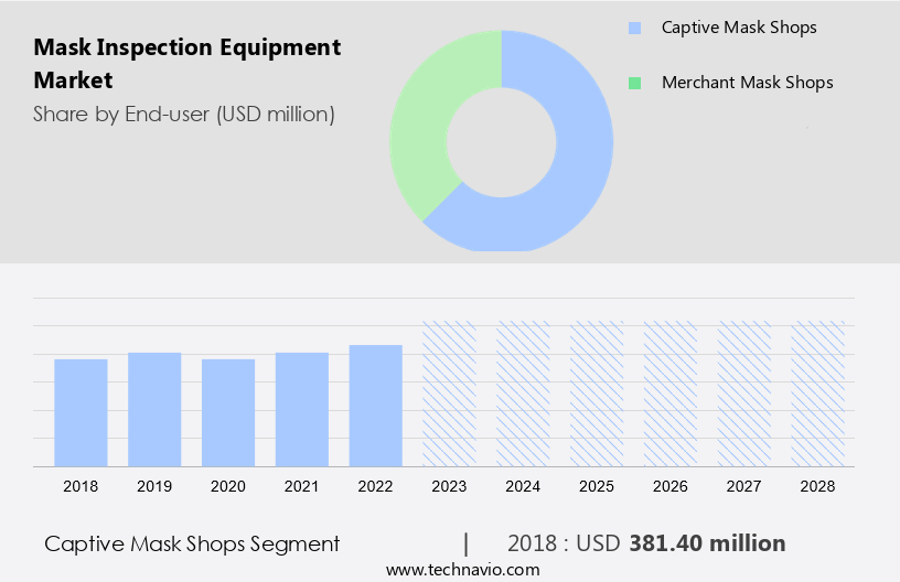
By End-user
The captive mask shops segment is estimated to witness significant growth during the forecast period. The photomask inspection tool market plays a crucial role in the semiconductor industry, particularly in the manufacture of semiconductor devices and consumer electronics. Photomasks, which are essential in the production of semiconductor wafers, undergo rigorous inspection using advanced inspection tools to ensure high-quality and zero-defect masks. Semiconductor demand, driven by various nations' policies and consumer electronics market trends, relies heavily on the semiconductor metrology inspection business.
Get a glance at the market share of various regions Download the PDF Sample
The captive mask shops segment was the largest and was valued at USD 381.40 million in 2018. High-volume manufacturing in fabrication facilities necessitates the use of cutting-edge metrology inspection tools for actinic inspection technology, absorber pattern inspection, and high-resolution, low-noise imaging. Die-to-Die (DB) and Semiconductor Device Manufacturers, as well as Mask Shops, rely on these tools to maintain resource utilization and address shortages of semiconductors caused by disruptions in semiconductor sourcing and international borders. The backlog of orders in the semiconductor industry underscores the importance of efficient inspection tools in ensuring timely delivery and maintaining a competitive edge.
Regional Analysis
For more insights on the market share of various regions Download PDF Sample now!
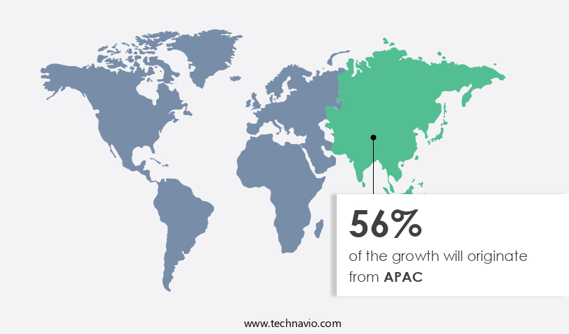
APAC is estimated to contribute 56% to the growth of the global market during the forecast period. Technavio’s analysts have elaborately explained the regional trends and drivers that shape the market during the forecast period. The market has witnessed a significant spike in expenditures due to the construction and expansion of IC fabrication facilities in semiconductor factories. Corporate design teams and pureplay foundries invest heavily in mask inspection equipment to ensure the production of high-quality ICs free from pattern flaws and faults. The cyclical nature of the semiconductor industry, driven by supply and demand dynamics, necessitates continuous innovation and investment in advanced mask inspection technologies. New fads in SiC fabrication and the integration of mask inspection in fabrication operations have added to the market's growth.
In addition, existing facilities are also upgrading their mask inspection capabilities to meet the increasing demand for semiconductor chips in various sectors, including data centers, servers, cloud storage devices, memory devices, automotive, healthcare, and industrial automation. The excess or deficit in the semiconductor chip market can significantly impact the market's trajectory. Overall, mask inspection plays a crucial role in maintaining the quality and reliability of electronic devices and ensuring their seamless integration into various applications.
Segment Overview
The market research report provides comprehensive data (region wise segment analysis), with forecasts and estimates in "USD million" for the period 2024 to 2028, as well as historical data from 2018 to 2022 for the following segments.
- End-user Outlook
- Captive mask shops
- Merchant mask shops
- Technology Outlook
- Optical
- E-beam
- Region Outlook
- North America
- The U.S.
- Canada
- South America
- Argentina
- Brazil
- Chile
- Europe
- U.K.
- Germany
- France
- Rest of Europe
- APAC
- China
- India
- Middle East & Africa
- Saudi Arabia
- South Africa
- Rest of the Middle East & Africa
- North America
You may also interested in below market reports:
- Face Mask Market by Channel, Type and Geography - Forecast and Analysis
- Venturi Mask Market Analysis North America, Europe, Asia, Rest of World (ROW) - US, Germany, Japan, China, UK - Size and Forecast
- Disposable Respirator Market Analysis North America, Europe, Asia, Rest of World (ROW) - US, Germany, China, France, Japan - Size and Forecast
Market Analyst Overview
The market plays a crucial role in the semiconductor industry by ensuring the production of high-quality semiconductor devices. This market caters to the inspection needs of semiconductor manufacturers, consumer electronics companies, and mask shops. Photomask inspection is a significant part of this market, focusing on the inspection of photomasks used in the manufacture of semiconductor wafers. Semiconductor demand, particularly in consumer electronics, drives the growth of this market. Semiconductor metrology, a critical aspect of semiconductor production, relies heavily on inspection equipment to maintain the desired level of quality. Nations implement policies to encourage semiconductor manufacturing, creating reliance on inspection equipment for semiconductor sourcing.
In addition, disruptions in semiconductor supply chains due to border closures and backlogs of orders have highlighted the importance of efficient resource utilization in the semiconductor industry. Cutting-edge metrology tools, such as actinic inspection technology, are essential for high-volume manufacturing in fabrication facilities. Zero-defect masks and defect inspection tools are integral to the inspection business. Absorber pattern inspection, with its high resolution and low noise imaging capabilities, is a growing area of focus. Die-to-Die (DB) inspection and Semiconductor Device Manufacturers also rely on advanced inspection tools for their production processes. In conclusion, the market plays a pivotal role in ensuring the production of high-quality semiconductor devices, particularly in the context of increasing semiconductor demand and the need for efficient resource utilization.
|
Market Scope |
|
|
Report Coverage |
Details |
|
Page number |
160 |
|
Base year |
2023 |
|
Historic period |
2018-2022 |
|
Forecast period |
2024-2028 |
|
Growth momentum & CAGR |
Accelerate at a CAGR of 7.08% |
|
Market growth 2024-2028 |
USD 305.2 million |
|
Market structure |
Concentrated |
|
YoY growth 2023-2024(%) |
6.48 |
|
Regional analysis |
APAC, North America, Europe, Middle East and Africa, and South America |
|
Performing market contribution |
APAC at 56% |
|
Key countries |
US, China, Japan, Germany, and France |
|
Competitive landscape |
Leading Companies, Market Positioning of Companies, Competitive Strategies, and Industry Risks |
|
Key companies profiled |
Applied Materials Inc., ASML, Bruker Corp., Carl Zeiss AG, HORIBA Ltd., JEOL Ltd, KLA Corp., Lasertec Corp, MueTec Automatisierte Mikroskopie und Messtechnik GmbH, Nanometrics Inc., Nikon Corp., NuFlare Technology Inc., and Planar Systems Inc. |
|
Market dynamics |
Parent market analysis, Market growth inducers and obstacles, Fast-growing and slow-growing segment analysis, COVID-19 impact and recovery analysis and future consumer dynamics, Market condition analysis for the market forecast period |
|
Customization purview |
If our market report has not included the data that you are looking for, you can reach out to our analysts and get segments customized. |
What are the Key Data Covered in this Market Research Report?
- CAGR of the market during the forecast period
- Detailed information on factors that will drive the market growth and forecasting between 2024 and 2028
- Precise estimation of the size of the market and its contribution of the market in focus to the parent market
- Accurate predictions about upcoming market growth and trends and changes in consumer behaviour
- Growth of the market across APAC, North America, Europe, Middle East and Africa, and South America
- Thorough analysis of the market’s competitive landscape and detailed information about companies
- Comprehensive analysis of factors that will challenge the growth of market companies
 RIA -
RIA - 
