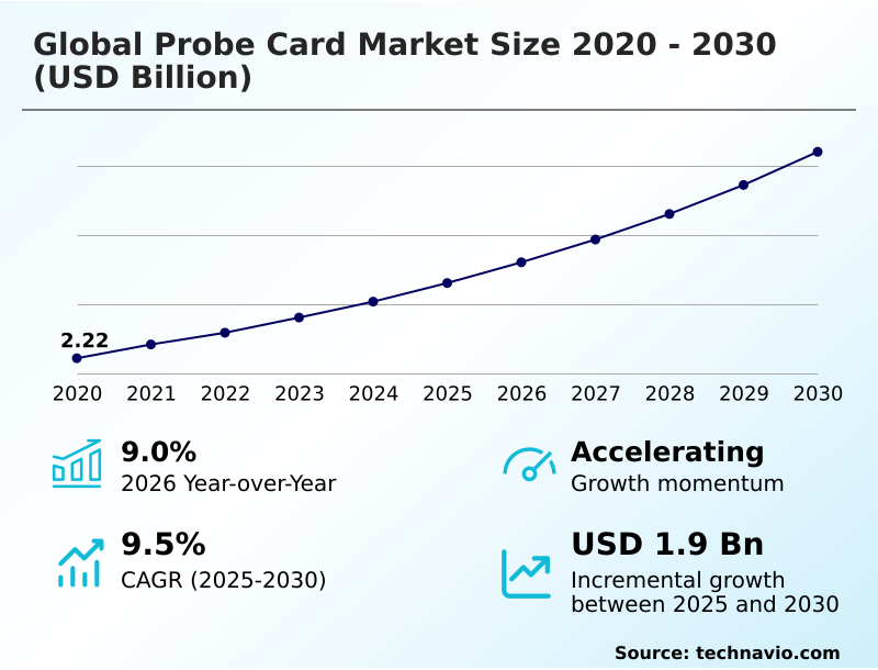
Probe Card Market Size 2026-2030
The probe card market size is valued to increase by USD 1.90 billion, at a CAGR of 9.5% from 2025 to 2030. Expansion of domestic semiconductor manufacturing and sovereign capacity initiatives will drive the probe card market.
Major Market Trends & Insights
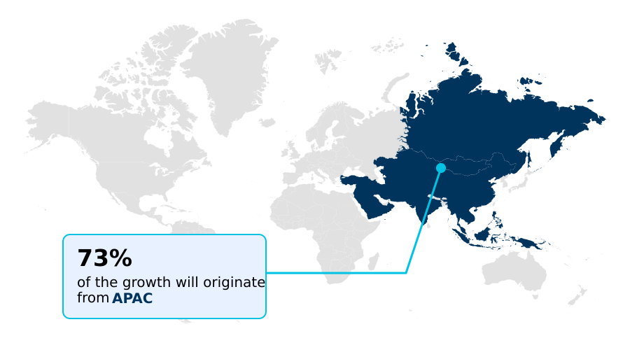
- APAC dominated the market and accounted for a 73% growth during the forecast period.
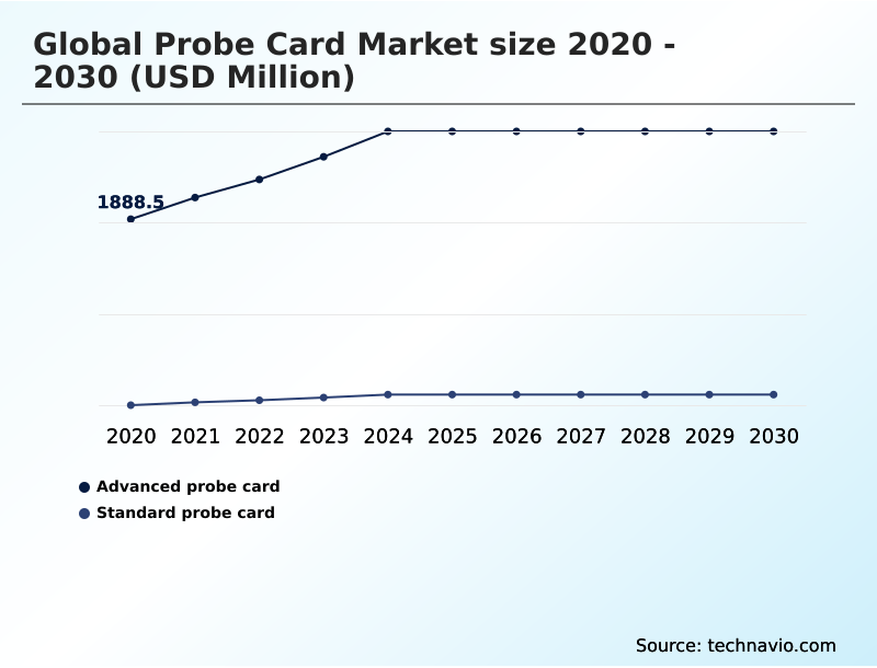
- By Product - Advanced probe card segment was valued at USD 2.62 billion in 2024
- By End-user - Foundry and logic segment accounted for the largest market revenue share in 2024
Market Size & Forecast
- Market Opportunities: USD 2.99 billion
- Market Future Opportunities: USD 1.90 billion
- CAGR from 2025 to 2030 : 9.5%
Market Summary
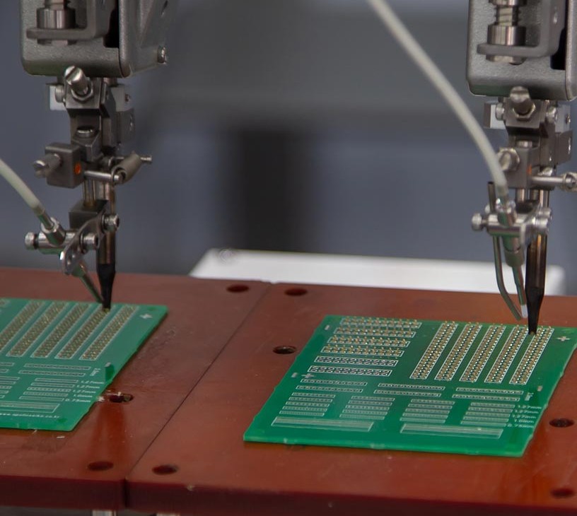
- The probe card market is the cornerstone of semiconductor yield management, functioning as the critical interface for wafer-level testing. As the industry transitions to advanced nodes for applications in AI and high-performance computing, the complexity of this electromechanical interface has grown exponentially.
- The demand is shifting from traditional cantilever designs to advanced MEMS-based and vertical probe architectures capable of high pin-count testing and fine-pitch probing. These advanced cards are essential for ensuring signal integrity validation during the electrical verification process.
- For instance, a fab manager overseeing production of a new automotive-grade power semiconductor must rely on high-voltage testing and high-current testing probe cards to identify defects early. Implementing a robust full-wafer contact strategy using these advanced tools can reduce test cycles and prevent faulty dies from entering the expensive packaging phase, directly improving profitability.
- This evolution is driven by the need to manage the escalating cost of test (CoT) reduction while ensuring the reliability of increasingly sophisticated micro-contact technology and chiplet-based architecture testing.
What will be the Size of the Probe Card Market during the forecast period?
Get Key Insights on Market Forecast (PDF) Get Free Sample
How is the Probe Card Market Segmented?
The probe card industry research report provides comprehensive data (region-wise segment analysis), with forecasts and estimates in "USD million" for the period 2026-2030, as well as historical data from 2020-2024 for the following segments.
- Product
- Advanced probe card
- Standard probe card
- End-user
- Foundry and logic
- Memory device
- Technology
- MEMS
- Vertical
- Cantilever
- Geography
- APAC
- China
- Japan
- South Korea
- North America
- US
- Canada
- Mexico
- Europe
- Germany
- UK
- France
- South America
- Brazil
- Argentina
- Middle East and Africa
- Saudi Arabia
- UAE
- South Africa
- Rest of World (ROW)
- APAC
By Product Insights
The advanced probe card segment is estimated to witness significant growth during the forecast period.
The advanced probe card segment is critical for next-generation semiconductor testing, driven by trends in AI, high-performance computing, and 5G.
These products, which primarily use MEMS fabrication and vertical probe architectures, are essential for addressing the stringent demands of wafer-level testing for devices built on leading-edge process nodes.
Their design supports superior parallelism, enabling the simultaneous testing of more dies and improving test throughput by up to 35%. This high-parallelism testing capability is crucial for managing the cost of test (CoT) reduction for complex chips.
As a result, this segment, which includes solutions for SoC testing and die testing, commands higher average selling prices and is projected to exhibit the strongest growth trajectory, directly mirroring the technological roadmap of leading semiconductor manufacturers.
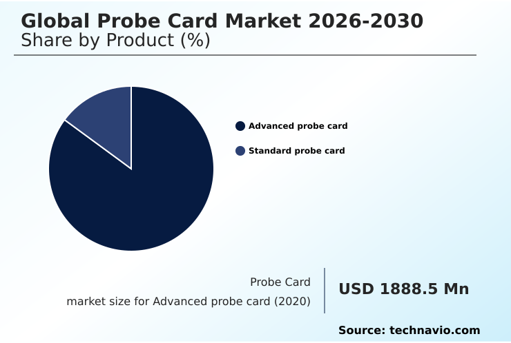
The Advanced probe card segment was valued at USD 2.62 billion in 2024 and showed a gradual increase during the forecast period.
Regional Analysis
APAC is estimated to contribute 73% to the growth of the global market during the forecast period.Technavio’s analysts have elaborately explained the regional trends and drivers that shape the market during the forecast period.
See How Probe Card Market Demand is Rising in APAC Get Free Sample
The geographic landscape of the probe card market is dominated by APAC, which represents over 70% of the global opportunity, driven by its high concentration of advanced foundries and memory manufacturers in countries like Taiwan, South Korea, and Japan.
This region's leadership in high-volume production creates sustained demand for solutions enabling test throughput optimization. Concurrently, government-led initiatives like the CHIPS acts in North America and Europe are reshaping the demand map by stimulating new fabrication projects.
These investments are increasing the need for localized probe card maintenance and repair capabilities and advanced solutions for fan-out wafer-level packaging tests, which are projected to increase regional demand by over 10%.
This strategic diversification aims to build resilient supply chains for critical components used in power semiconductor testing.
Market Dynamics
Our researchers analyzed the data with 2025 as the base year, along with the key drivers, trends, and challenges. A holistic analysis of drivers will help companies refine their marketing strategies to gain a competitive advantage.
- The market is evolving to meet highly specific application needs, creating demand for a diverse range of specialized products. The development of an advanced probe card for AI accelerators, for example, is critical for validating the performance of complex processors. Similarly, the probe card for high bandwidth memory testing must handle massive parallelism and stringent thermal requirements.
- The industry's push toward sub-5nm nodes has made the MEMS probe card for 2nm process technology an essential development area. In parallel, the automotive and industrial sectors drive the need for vertical probe cards for power semiconductor testing, including solutions for GaN and SiC wafer testing.
- The rise of heterogeneous integration and advanced packaging is fueling requirements for a probe card for wafer-level chip-scale packaging and a testing solution for automotive microcontrollers. New optical technologies require a probe card solutions for co-packaged optics, while high-speed digital applications demand a signal integrity probe card for high-speed digital validation.
- Reducing cost of test with vertical probe cards remains a key strategy for mature nodes, alongside using a cantilever probe for low pin count analog ICs. Other specialized solutions include a high-temperature probe card for power electronics, a low-leakage probe card for parametric testing, and a custom probe card for medical sensor ICs.
- Achieving full-wafer contact for DRAM testing can reduce test cycles by over 50% compared to legacy partial-wafer methods, demonstrating a clear link between advanced testing interfaces for heterogeneous integration and operational efficiency. This specialization is also evident in the need for a probe card for stacked die 3D IC validation and a probe card for fine-pitch SOC devices.
What are the key market drivers leading to the rise in the adoption of Probe Card Industry?
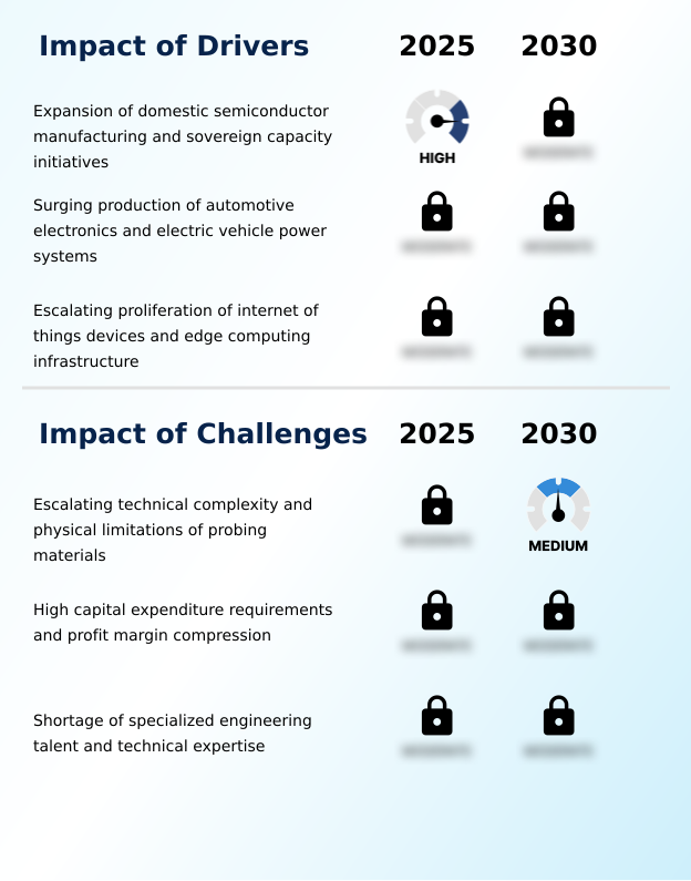
- The expansion of domestic semiconductor manufacturing, propelled by sovereign capacity initiatives, is a primary driver fueling market growth.
- Market growth is significantly propelled by the global expansion of domestic semiconductor manufacturing, supported by government initiatives aiming to secure sovereign supply chains. This creates a surge in demand for wafer-level testing infrastructure, particularly for MEMS-based probing solutions.
- The electrification of vehicles is another primary catalyst, as automotive electronics require rigorous, automotive-grade testing solutions that increase reliability by more than three times compared to consumer-grade standards.
- The proliferation of IoT devices and edge computing further fuels demand, requiring high-throughput, multi-site testing for a diverse range of low-power chips.
- These drivers ensure a consistent need for advanced probe cards to support high-parallelism testing, thermal management in testing, and overall wafer mapping.
What are the market trends shaping the Probe Card Industry?
- The proliferation of high-performance computing and artificial intelligence integration is a key trend. This is reshaping testing requirements and driving demand for advanced probe card solutions.
- The market is undergoing a significant transformation driven by the growth of high-performance computing and AI, which demands advanced solutions for 2nm process node tests. This trend is pushing the adoption of MEMS-based probing, which offers superior precision for testing complex devices, reducing setup times by over 20% compared to traditional methods.
- The rise of advanced packaging test requirements, driven by chiplet-based architectures, necessitates probe cards that can handle intricate interconnects. Furthermore, the integration of high-performance chips in data centers fuels the need for rigorous wafer-level testing with high-frequency RF testing capabilities.
- These technological shifts, including a focus on yield management and high-voltage testing, are evolving the market into a high-technology sector where R&D investment is paramount.
What challenges does the Probe Card Industry face during its growth?
- A key market challenge stems from the escalating technical complexity and inherent physical limitations of advanced probing materials.
- The market faces considerable challenges as semiconductor features shrink, increasing the technical complexity of electromechanical interfaces. The physical limitations of probe needle material for fine-pitch probing can lead to a 10% increase in test-related scrap if not properly managed. High capital expenditure for MEMS fabrication and the compression of profit margins due to customer price sensitivity present significant economic hurdles.
- The transition to vertical probe architecture involves massive investments, creating high barriers to entry. Additionally, a persistent shortage of specialized engineering talent capable of designing and maintaining hardware for tasks like probe-to-pad alignment and high pin-count testing limits the industry's ability to scale, delaying development cycles by up to six months in some cases.
Exclusive Technavio Analysis on Customer Landscape
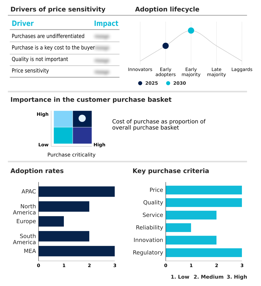
The probe card market forecasting report includes the adoption lifecycle of the market, covering from the innovator’s stage to the laggard’s stage. It focuses on adoption rates in different regions based on penetration. Furthermore, the probe card market report also includes key purchase criteria and drivers of price sensitivity to help companies evaluate and develop their market growth analysis strategies.
Customer Landscape of Probe Card Industry
Competitive Landscape
Companies are implementing various strategies, such as strategic alliances, probe card market forecast, partnerships, mergers and acquisitions, geographical expansion, and product/service launches, to enhance their presence in the industry.
Advantest Corp. - Offerings include advanced wafer-level testing solutions, featuring cantilever, MEMS, and RF probe cards for comprehensive semiconductor validation and characterization.
The industry research and growth report includes detailed analyses of the competitive landscape of the market and information about key companies, including:
- Advantest Corp.
- Apollo Wave Corp
- Celadon Systems Inc.
- Chunghwa Precision Test Tech
- Cohu Inc.
- DGT Technology
- Feinmetall GmbH
- FormFactor Inc.
- Korea Instrument Co. Ltd.
- MaxOne Semiconductor
- Micronics Japan Co. Ltd.
- MPI Corp.
- Nidec SV Probe
- Shenzhen Sestos Technology
- Star Quest Technologies Pte Ltd.
- Synergie Cad
- Technoprobe S.p.A.
- TSE Co. Ltd.
- Wentworth Laboratories Ltd.
- Will Technology Co. Ltd.
Qualitative and quantitative analysis of companies has been conducted to help clients understand the wider business environment as well as the strengths and weaknesses of key industry players. Data is qualitatively analyzed to categorize companies as pure play, category-focused, industry-focused, and diversified; it is quantitatively analyzed to categorize companies as dominant, leading, strong, tentative, and weak.
Recent Development and News in Probe card market
- In January 2025, Advantest Corp. announced strategic minority investments in Technoprobe S.p.A. and FormFactor Inc. to advance technology development for high-performance, total testing solutions.
- In March 2025, Micron Technology announced a major expansion of its research and manufacturing operations in New York, a long-term project focused on producing advanced memory chips that will drive future demand for high-volume probe cards.
- In April 2025, FormFactor Inc. announced the strategic acquisition of Keystone Photonics to enhance its capabilities in the expanding market for co-packaged optics testing solutions.
- In May 2025, Micronics Japan Co. Ltd. revealed it had achieved primary supplier qualification from TSMC for its upcoming 2-nanometer process technology, following an extensive 18-month co-development program.
Dive into Technavio’s robust research methodology, blending expert interviews, extensive data synthesis, and validated models for unparalleled Probe Card Market insights. See full methodology.
| Market Scope | |
|---|---|
| Page number | 285 |
| Base year | 2025 |
| Historic period | 2020-2024 |
| Forecast period | 2026-2030 |
| Growth momentum & CAGR | Accelerate at a CAGR of 9.5% |
| Market growth 2026-2030 | USD 1897.5 million |
| Market structure | Fragmented |
| YoY growth 2025-2026(%) | 9.0% |
| Key countries | Taiwan, China, Japan, South Korea, India, Australia, US, Canada, Mexico, Germany, UK, France, Italy, Spain, The Netherlands, Brazil, Argentina, Chile, Saudi Arabia, UAE, South Africa, Israel and Turkey |
| Competitive landscape | Leading Companies, Market Positioning of Companies, Competitive Strategies, and Industry Risks |
Research Analyst Overview
- The probe card market is defined by its role as a critical electromechanical interface in the semiconductor wafer sort process. Its evolution is tied to the increasing complexity of integrated circuits, demanding continuous innovation in MEMS-based probing and vertical probe architecture.
- The industry is moving beyond simple die testing to address the challenges of 3D IC testing and advanced packaging tests. The adoption of multi-site testing, for example, directly impacts boardroom decisions on capital expenditure, as it requires significant investment in compatible automated test equipment (ATE) interfaces but can improve first-pass yields by up to 5%.
- Achieving precise probe-to-pad alignment and mastering micro-contact technology are essential for high pin-count testing and fine-pitch probing. Key technologies enabling this progress include full-wafer contact for memory and high-frequency RF testing for wireless components.
- As device complexity grows, so does the importance of parametric testing, signal integrity validation, and specialized power semiconductor testing to ensure reliability from the foundry to the final product, covering both SoC testing and heterogeneous integration testing with MEMS fabrication and advanced probe needle material.
What are the Key Data Covered in this Probe Card Market Research and Growth Report?
-
What is the expected growth of the Probe Card Market between 2026 and 2030?
-
USD 1.90 billion, at a CAGR of 9.5%
-
-
What segmentation does the market report cover?
-
The report is segmented by Product (Advanced probe card, and Standard probe card), End-user (Foundry and logic, and Memory device), Technology (MEMS, Vertical, and Cantilever) and Geography (APAC, North America, Europe, South America, Middle East and Africa)
-
-
Which regions are analyzed in the report?
-
APAC, North America, Europe, South America and Middle East and Africa
-
-
What are the key growth drivers and market challenges?
-
Expansion of domestic semiconductor manufacturing and sovereign capacity initiatives, Escalating technical complexity and physical limitations of probing materials
-
-
Who are the major players in the Probe Card Market?
-
Advantest Corp., Apollo Wave Corp, Celadon Systems Inc., Chunghwa Precision Test Tech, Cohu Inc., DGT Technology, Feinmetall GmbH, FormFactor Inc., Korea Instrument Co. Ltd., MaxOne Semiconductor, Micronics Japan Co. Ltd., MPI Corp., Nidec SV Probe, Shenzhen Sestos Technology, Star Quest Technologies Pte Ltd., Synergie Cad, Technoprobe S.p.A., TSE Co. Ltd., Wentworth Laboratories Ltd. and Will Technology Co. Ltd.
-
Market Research Insights
- The market is shaped by a focus on operational efficiency, with advanced solutions enabling test cell utilization improvements of over 20%. The adoption of high-parallelism testing methodologies is directly linked to achieving a 15% cost of test (CoT) reduction for high-volume memory device testing. Furthermore, a strategic emphasis on probe card maintenance and repair extends equipment life, lowering capital expenditure.
- These dynamics, including the shift toward advanced node testing and automotive-grade testing solutions, highlight a market where technical capability directly translates into measurable financial and operational gains for semiconductor manufacturers. The need to support system-level testing and non-memory device testing further diversifies technical requirements.
We can help! Our analysts can customize this probe card market research report to meet your requirements.
 RIA -
RIA - 
