Fan-Out Wafer Level Packaging Market Size 2025-2029
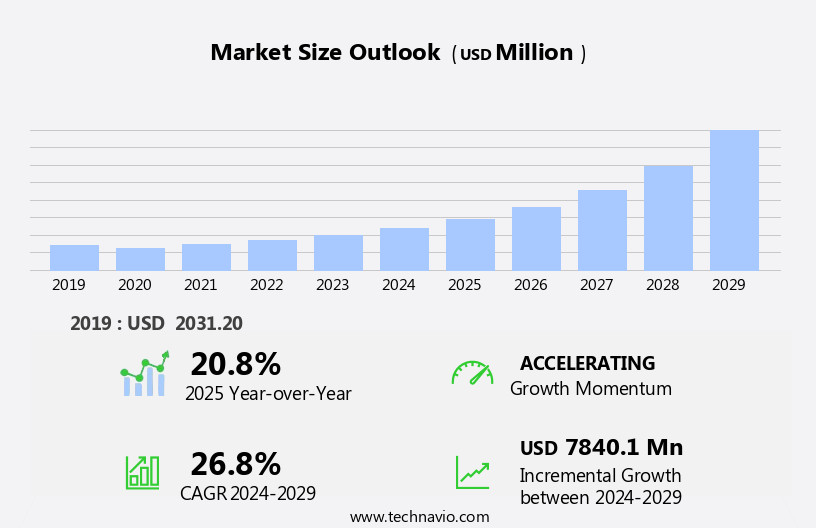
The fan-out wafer level packaging market size is forecast to increase by USD 7.84 billion, at a CAGR of 26.8% between 2024 and 2029.
- The market is experiencing significant growth due to the increasing demand for compactly designed electronics in various industries, including consumer electronics, data centers, renewable energy, and autonomous vehicles. One of the key trends driving this growth is the increasing adoption of semiconductor ICs in automobiles, leading to the need for advanced packaging solutions like FOWLP. However, the market also faces challenges such as increased production costs due to warpage, which can impact the yield and quality of the packaged semiconductors.
- In the consumer electronics sector, the demand for smaller, more powerful devices is driving the need for FOWLP, while in data centers, the requirement for high-performance, power-efficient components are fueling growth. The mobile phone industry is also expected to contribute significantly to the market's growth, as manufacturers seek to incorporate more advanced features into their devices while maintaining compact form factors. Overall, the FOWLP market is poised for significant growth In the coming years, driven by these trends and the increasing demand for compact, high-performance electronics across various industries.
What will be the Size of the Fan-Out Wafer Level Packaging Market During the Forecast Period?
- The market within the semiconductor-based technologies sector experiences continuous growth due to the increasing demand for footprint-sensitive devices, such as advanced consumer electronics like smartwatches and ultra-thin portable devices. FOWLP offers advantages like package-on-package (PoP) and memory-on-logic solutions, which cater to the needs of high-performing ICs In these applications. Artificial intelligence and machine learning technologies are driving the adoption of advanced packaging solutions, including FOWLP, due to their requirements for increased integration and miniaturization.
- FOWLP addresses thermal issues associated with traditional packaging methods by enabling wafer-level processes, reducing manufacturing costs, and enabling heterogeneous integration. IC packaging technology, including FOWLP, plays a crucial role In the consumer electronics sector, particularly In the production of multichip packages for smartwatches, laptops, and other advanced electronic devices. As the demand for smaller, more powerful, and energy-efficient devices continues to grow, the FOWLP market is expected to expand further, providing significant opportunities for innovation and growth.
How is this Fan-Out Wafer Level Packaging Industry segmented and which is the largest segment?
The fan-out wafer level packaging industry research report provides comprehensive data (region-wise segment analysis), with forecasts and estimates in "USD billion" for the period 2025-2029, as well as historical data from 2019-2023 for the following segments.
- Technology
- High density
- Standard density
- Type
- 200 mm
- 300 mm
- Panel
- Application
- Consumer electronics
- Automotive
- Defense and aerospace
- Medical
- Others
- Product Type
- Fan-out WLP
- Through silicon via
- Integrated passive device
- Fan-in WLP
- Geography
- APAC
- China
- Japan
- South Korea
- Singapore
- North America
- Canada
- US
- Europe
- Germany
- UK
- South America
- Brazil
- Middle East and Africa
- APAC
By Technology Insights
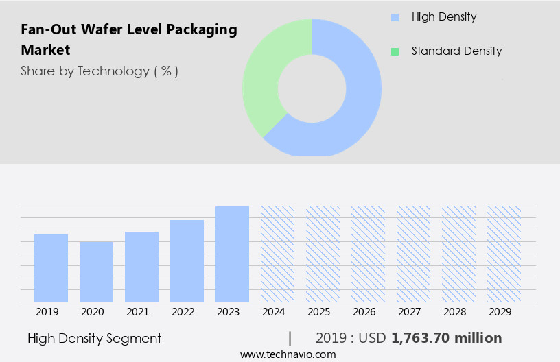
The high density segment is estimated to witness significant growth during the forecast period. Fan-out wafer level packaging (FoWLP) is a high-density semiconductor packaging technology featuring over 200 external I/Os and less than 8m line/space. This technology is increasingly adopted for mid-to-high-end applications, particularly in application processor engines (APEs) with higher I/O requirements. The integration of neural network processor (NNU) architecture in CPUs, GPUs, DSPs, and FPGAs is driving the demand for FoWLP. Furthermore, the growing investments in high-performance computing and the demand for high-bandwidth memory (HBM) will propel semiconductor packaging companies to implement advanced packaging solutions for high-performance application processors, CPUs, and FPGAs used in data centers and high-performance computing applications. Machine learning, UHD fan-out technology, and advanced design flexibility are other factors contributing to the long-term impact of FoWLP.
Companies such as Changdian Technology, Chip heterogeneous integration, and Mega pillar plating are at the forefront of FoWLP innovation. This technology is essential for compact electronic devices, including microcontrollers, power modules, and stacked die designs, in various industries, including automotive, artificial intelligence, biotechnology, and telecommunications. Despite the complex manufacturing process and thermal issues, FoWLP offers significant benefits, such as energy efficiency, thermal resistance, and customary chip-scale packaging solutions.
Get a glance at the market report of share of various segments Request Free Sample
The high density segment was valued at USD 1.76 billion in 2019 and showed a gradual increase during the forecast period.
Regional Analysis
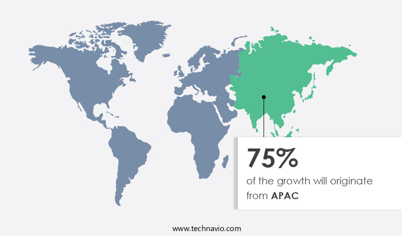
APAC is estimated to contribute 75% to the growth of the global market during the forecast period. Technavio's analysts have elaborately explained the regional trends and drivers that shape the market during the forecast period.
For more insights on the market size of various regions, Request Free Sample
The market in APAC is driven by the presence of major foundries and OSAT companies, such as nepes and ChangDian Technology Co. Ltd. ASE Technology Holding Co. Ltd. Is a leading manufacturer of fan-out packaging, offering two categories: Chip-First and Chip-Last. Chip-First is ideal for FPGAs, GPUs, networking, RF modules, and PA modules, reducing power loss and thermal dissipation. Fan-out packaging technology's strong mechanism caters to various applications, including FPGAs, GPUs, networking, RF modules, and PA modules. This technology is crucial for manufacturing high-performance computing components, such as FPGAs and GPUs, which require high-density interconnects and low thermal resistance. Additionally, fan-out packaging is beneficial for power electronics applications due to its ability to minimize power loss and thermal dissipation.
The technology's advanced design flexibility and compact design make it suitable for micro-electro-mechanical systems (MEMS), microcontrollers, power modules, and stacked die designs. Furthermore, fan-out packaging is essential for ultra-thin portable devices, wearable electronics, and smartwatches, which require high-performance, energy-efficient, and miniaturized packaged ICs. The technology's electrical performance, dielectric structure, and radio frequency devices' compatibility make it suitable for various applications, including in-vehicle infotainment (IVI), engine control units, communication modules, and autonomous vehicles. The fan-out packaging market's long-term impact is significant, as it addresses thermal issues and improves device efficiency, yield rates, and manufacturing costs.
Market Dynamics
Our researchers analyzed the data with 2024 as the base year, along with the key drivers, trends, and challenges. A holistic analysis of drivers will help companies refine their marketing strategies to gain a competitive advantage.
What are the key market drivers leading to the rise In the adoption of Fan-Out Wafer Level Packaging Industry?
- Increased demand for compactly designed electronics is the key driver of the market. The semiconductor industry's ongoing advancements in technologies are fueling the demand for miniaturized electronic components. The integration of Human-Machine Interface (HMI) technologies, wireless communication advancements, and telecommunication standards development are significant factors driving this trend. Miniaturized semiconductor components, including RF devices, wireless modules, and application processors, can be integrated into various devices such as smartphones, healthcare equipment, and automobiles. The miniaturization of semiconductor Integrated Circuits (ICs) and the integration of multiple functions within a single IC are leading to the development of ICs based on lower technology nodes, such as 14 nm, 10 nm, 7 nm, and below. This trend is crucial for industries like automotive, where footprint-sensitive devices, such as Memory-on-Logic solutions and Package-on-Package (PoP), are increasingly being adopted for advanced applications like Autonomous cars, AI chips, and In-vehicle infotainment (IVI).
- Moreover, the semiconductor manufacturing industry is focusing on advanced packaging techniques like Fan-Out packaging, Chip heterogeneous integration, and High-Density Fan-Out, to address thermal issues and improve device efficiency. Technologies like UHD fan-out, Mega pillar plating, and Changdian Technology are gaining popularity due to their ability to address challenges like differential shrinkage and reduced lifespan. In addition, the increasing demand for high-performance computing, compact design, and energy-efficient solutions is driving the adoption of advanced packaging technologies. These technologies enable the production of miniaturized packaged ICs, which are essential for various industries, including telecommunications, consumer electronics, and automotive. Furthermore, the semiconductor supply chain is undergoing significant changes, with a shift towards just-in-time production schedules and low inventory levels to minimize costs and improve delivery timelines.
What are the market trends shaping the Fan-Out Wafer Level Packaging Industry?
- Increasing adoption of semiconductor ICs in automobiles is the upcoming market trend. The market is experiencing significant growth due to the increasing adoption of footprint-sensitive devices, such as package-on-package (PoP) and memory-on-logic solutions, in various industries. In the automotive sector, this trend is driven by the shift towards electric, autonomous, and connected vehicles. Companies like Audi and General Motors are investing in advanced technologies like Ultra-High Density (UHD) fan-out technology, mega pillar plating, and chip heterogeneous integration for high-performance computing applications. The use of machine learning algorithms In the cloud, autonomous cars, and AI chips is fueling the demand for compact, energy-efficient, and high-performing ICs. The semiconductor supply chain is adapting to these changes by implementing advanced packaging technologies like fan-out packaging, which offers improved electrical performance, thermal resistance, and interconnect solutions.
- However, this complex manufacturing process comes with challenges such as thermal issues, differential shrinkage, and reduced lifespan. To mitigate these risks, semiconductor manufacturing companies are focusing on improving manufacturing costs, yield rates, and quality control measures. Additionally, the adoption of advanced design flexibility, such as stacked die designs and silicon process technology, is enabling the production of miniaturized packaged ICs for compact electronic devices like smartwatches and wearable electronics. The semiconductor industry is also witnessing the emergence of new markets, such as Mega pillar plating, Changdian Technology, and protected fan-out technology, which offer enhanced performance and reliability for light-sensitive devices and radio frequency devices.
What challenges does the Fan-Out Wafer Level Packaging Industry face during its growth?
- Increased production costs because of warpage is a key challenge affecting the industry growth. The market faces challenges due to the issue of warpage, which increases production costs. Warpage refers to the distortion of the molded part's surface not adhering to the intended design shape. This deformation of the wafer surface results in wasted wafers and higher manufacturing costs. The primary cause of warpage is differential shrinkage during the packaging process, leading to an uneven, compact shape. This issue arises multiple times during fan-out wafer level packaging, potentially impacting long-term market growth. In fan-out packaging, the chip surface is connected to external I/Os using conductive traces and an epoxy mold compound. Advanced packaging technologies, such as High-Density Fan-Out, Mega pillar plating, and chip heterogeneous integration, require high precision and complex manufacturing processes.
- These technologies are used in various applications, including high-performance computing, memory-on-logic solutions, and package-on-package (PoP) solutions. The market is influenced by various factors, including the semiconductor supply chain, production schedules, and quality control measures. The demand for fan-out packaging is driven by the need for compact design, energy efficiency, and high-performance in various industries, such as automotive, artificial intelligence, and biotechnology. However, thermal issues and yield rates are critical challenges that must be addressed to ensure the long-term impact of fan-out wafer level packaging.
- Fan-out wafer level packaging is used in various applications, including micro-electro-mechanical systems (MEMS), pressure sensors, gyroscopes, and autonomous vehicles. The market is expected to grow as the demand for miniaturized packaged ICs and compact electronic devices increases. The use of fan-out packaging in advanced design flexibility, physical performance, and high-power applications is also a significant trend. However, the complex manufacturing process and potential for silicon cracking and chipping during the packaging process necessitate protected fan-out technology to mitigate the risk of damage.
Exclusive Customer Landscape
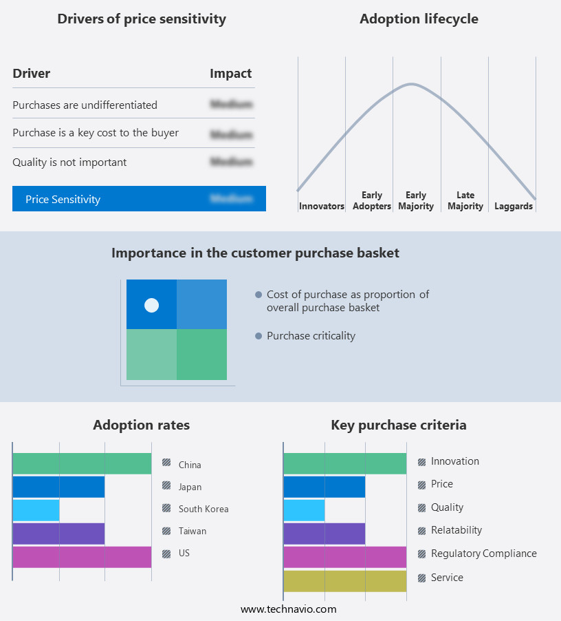
The fan-out wafer level packaging market forecasting report includes the adoption lifecycle of the market, covering from the innovator's stage to the laggard's stage. It focuses on adoption rates in different regions based on penetration. Furthermore, the fan-out wafer level packaging market report also includes key purchase criteria and drivers of price sensitivity to help companies evaluate and develop their market growth analysis strategies.
Customer Landscape
Key Companies & Market Insights
Companies are implementing various strategies, such as strategic alliances, fan-out wafer level packaging market forecast, partnerships, mergers and acquisitions, geographical expansion, and product/service launches, to enhance their presence In the industry.
Amkor Technology Inc. - The company offers fan out wafer level packaging schemes for System in Package or SIP and chip scale to 3D systems.
The industry research and growth report includes detailed analyses of the competitive landscape of the market and information about key companies, including:
- ASE Technology Holding Co. Ltd.
- Deca Technologies Inc.
- Infineon Technologies AG
- Jiangsu Changdian Technology Co. Ltd.
- nepes Corp.
- Nordson Corp.
- NXP Semiconductors NV
- Onto Innovation Inc.
- Panasonic Holdings Corp.
- Powertech Technology Inc.
- Renesas Electronics Corp.
- Singapore Semiconductor Industry Association
- SUSS MICROTEC SE
- Taiwan Semiconductor Manufacturing Co. Ltd.
- Unisem M Berhad
- UTAC Holdings Ltd.
- Winbond Electronics Corp.
- Yield Engineering Systems
- Yole Developpement SA
Qualitative and quantitative analysis of companies has been conducted to help clients understand the wider business environment as well as the strengths and weaknesses of key industry players. Data is qualitatively analyzed to categorize companies as pure play, category-focused, industry-focused, and diversified; it is quantitatively analyzed to categorize companies as dominant, leading, strong, tentative, and weak.
Research Analyst Overview
The market encompasses a range of semiconductor-based technologies that cater to the increasing demand for footprint-sensitive devices and advanced packaging solutions. These technologies include package-on-package (PoP) and memory-on-logic solutions, which enable the integration of multiple chips into a single package, thereby reducing the overall footprint and improving performance. The adoption of FOWLP is driven by several factors, including the growing prevalence of machine learning, artificial intelligence (AI), and the cloud. The proliferation of these technologies in various industries, such as autonomous cars and biotechnology, necessitates the development of high-density fan-out solutions that can accommodate the complex interconnects and thermal management requirements of these applications.
Further, UHD fan-out technology is a key enabler of these advanced packaging solutions. This technology employs mega pillar plating and chip heterogeneous integration to create high-performance computing systems with minimal thermal issues. Changdian technology and other advanced packaging methods are also gaining traction In the market due to their ability to address the challenges associated with traditional packaging methods, such as manufacturing costs, yield rates, and complex manufacturing processes. The semiconductor supply chain is undergoing significant changes due to the increasing demand for FOWLP solutions. Production schedules are becoming more dynamic, and quality control measures are being implemented to ensure the delivery of high-quality, efficient devices.
In addition, the movement of goods is also becoming more streamlined, with a focus on reducing inventory levels and optimizing the supply chain to meet the demands of the market. The FOWLP market is characterized by its complex manufacturing process, which involves the deposition of conductive traces on the chip surface and the encapsulation of the chips in epoxy mold compound. This process requires advanced design flexibility and physical performance to accommodate the varying requirements of different applications. The adoption of FOWLP is also driving innovation in various industries. For instance, In the automotive sector, FOWLP solutions are being used to develop high-performing, energy-efficient power modules and microcontrollers for in-vehicle infotainment (IVI) systems, engine control units, communication modules, and other smart automotive solutions.
|
Market Scope |
|
|
Report Coverage |
Details |
|
Page number |
253 |
|
Base year |
2024 |
|
Historic period |
2019-2023 |
|
Forecast period |
2025-2029 |
|
Growth momentum & CAGR |
Accelerate at a CAGR of 26.8% |
|
Market Growth 2025-2029 |
USD 7.84 billion |
|
Market structure |
Fragmented |
|
YoY growth 2024-2025(%) |
20.8 |
|
Key countries |
Taiwan, South Korea, China, US, Japan, Singapore, Canada, Germany, UK, and Brazil |
|
Competitive landscape |
Leading Companies, Market Positioning of Companies, Competitive Strategies, and Industry Risks |
What are the Key Data Covered in this Fan-Out Wafer Level Packaging Market Research and Growth Report?
- CAGR of the Fan-Out Wafer Level Packaging industry during the forecast period
- Detailed information on factors that will drive the market growth and forecasting between 2025 and 2029
- Precise estimation of the size of the market and its contribution of the industry in focus to the parent market
- Accurate predictions about upcoming growth and trends and changes in consumer behaviour
- Growth of the market across APAC, North America, Europe, South America, and Middle East and Africa
- Thorough analysis of the market's competitive landscape and detailed information about companies
- Comprehensive analysis of factors that will challenge the fan-out wafer level packaging market growth of industry companies
We can help! Our analysts can customize this fan-out wafer level packaging market research report to meet your requirements.
 RIA -
RIA - 
