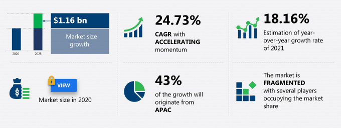
The e-beam wafer inspection system market share is expected to increase by USD 1.16 billion from 2020 to 2025, and the market’s growth momentum will accelerate at a CAGR of 24.73%.
This e-beam wafer inspection system market research report provides valuable insights on the post COVID-19 impact on the market, which will help companies evaluate their business approaches. Furthermore, this report extensively covers e-beam wafer inspection system market segmentation by end user (IDM and foundry) and geography (APAC, North America, Europe, South America, and MEA). The e-beam wafer inspection system market report also offers information on several market vendors, including Applied Materials Inc., ASML Holding NV, Cognex Corp., Hitachi Ltd., JEOL Ltd., KLA Corp., Nanotronics, Newport Corp., Onto Innovation Inc., and Photo electron Soul Inc. among others.
What will the E-Beam Wafer Inspection System Market Size be During the Forecast Period?
Download the Free Report Sample to Unlock the E-Beam Wafer Inspection System Market Size for the Forecast Period and Other Important Statistics
E-Beam Wafer Inspection System Market: Key Drivers, Trends, and Challenges
Based on our research output, there has been a negative impact on the market growth during and post COVID-19 era. The increasing demand for semiconductor wafers is notably driving the e-beam wafer inspection system market growth, although factors such as difficulty in finding defects in an embedded chip may impede the market growth. Our research analysts have studied the historical data and deduced the key market drivers and the COVID-19 pandemic impact on the e-beam wafer inspection system industry. The holistic analysis of the drivers will help in deducing end goals and refining marketing strategies to gain a competitive edge.
Key E-Beam Wafer Inspection System Market Driver
Increasing demand for semiconductor wafers is a major driver fueling the e-beam wafer inspection system market growth. There has been an increase in the adoption of certain communication devices and consumer electronic equipment such as smartphones, tablets, wearables, LCDs, LEDs, and solid-state drives (SSD), owing to the demand for advanced and sophisticated electronic products from consumers worldwide. This has indirectly led to the high demand for superior quality semiconductors such as silicon-based wafers, which play a key role in ICs. Such ICs are an integral part of many electronic devices such as mobiles and computers. Similarly, new and emerging technologies such as the Internet of Things (IoT), machine-to-machine (M2M), ultra high definition (UHD) televisions, hybrid laptops, and vehicle automation are further driving the demand for semiconductor wafers. Therefore, as the demand for semiconductor wafers increases, the need for wafer inspection systems also increases in order to keep a check on the process and quality of the wafers. The increasing demand for semiconductor wafers will have a high impact on semiconductor foundries, as these foundries will invest in boosting their production capacity either by the expansion of the existing fabs or by developing new fabs.
Key E-Beam Wafer Inspection System Market Trend
Multi-beam e-beam inspection is a major trend influencing the e-beam wafer inspection system market growth. The e-beam wafer inspection system market is of two types, one being the traditional e-beam inspection and the other being the multi-beam e-beam inspection. To increase the throughputs of e-beam inspection systems, researchers are working to develop a multi-beam e-beam inspection system, which would make the throughputs faster than the traditional e-beam inspection system. These systems are expected to be launched during the forecast period and will take quite some time for mass production as these are still under development. For instance, in May 2020, ASML Holding NV (ASML) completed system integration and testing of its first-generation HMI multibeam inspection (MBI) system for 5 nm nodes and beyond. The HMI eScan 1000 demonstrated successful multibeam operation, simultaneously scanning nine beams on several test wafers. With nine beams, the eScan 1000 will increase throughput up to 600% compared to single e-beam inspection tools for targeted in-line defect inspection applications.
Key E-Beam Wafer Inspection System Market Challenge
The difficulty in finding defects in an embedded chip is a major hindrance to the e-beam wafer inspection system market growth. As the chips are embedded with a dynamic random-access memory (DRAM), static random-access memory (SRAM), and dense logic, it becomes difficult to find the defects. The chips are filled with minute materials, and it becomes hard to list out the part in which the defect is present. There is also some confusion regarding nuisance in the wafer and the actual defect of interest (DOI). A nuisance is a small irregularity in the wafer, which is not classified as a defect or impurity. In advanced nodes, the nuisances and DOIs are bunched together on a map and hence cannot be distinguished, which is a major challenge for the R&D teams of inspection system vendors. Hence, these challenges to identify defects on embedded chips can negatively affect the demand for e-beam wafer inspection systems for embedded chip applications and thereby hinder the potential growth of the market during the forecast period.
This e-beam wafer inspection system market analysis report also provides detailed information on other upcoming trends and challenges that will have a far-reaching effect on the market growth. The actionable insights on the trends and challenges will help companies evaluate and develop growth strategies for 2021-2025.
Parent Market Analysis
Technavio categorizes the global e-beam wafer inspection system market as a part of the global semiconductor equipment market. Our research report has extensively covered external factors influencing the parent market growth potential in the coming years, which will determine the levels of growth of the e-beam wafer inspection system market during the forecast period.
Who are the Major E-Beam Wafer Inspection System Market Vendors?
The report analyzes the market’s competitive landscape and offers information on several market vendors, including:
- Applied Materials Inc.
- ASML Holding NV
- Cognex Corp.
- Hitachi Ltd.
- JEOL Ltd.
- KLA Corp.
- Nanotronics
- Newport Corp.
- Onto Innovation Inc.
- Photo electron Soul Inc.
This statistical study of the e-beam wafer inspection system market encompasses successful business strategies deployed by the key vendors. The e-beam wafer inspection system market is fragmented and the vendors are deploying organic and inorganic growth strategies to compete in the market.
To make the most of the opportunities and recover from post COVID-19 impact, market vendors should focus more on the growth prospects in the fast-growing segments, while maintaining their positions in the slow-growing segments.
The e-beam wafer inspection system market forecast report offers in-depth insights into key vendor profiles. The profiles include information on the production, sustainability, and prospects of the leading companies.
E-Beam Wafer Inspection System Market Value Chain Analysis
Our report provides extensive information on the value chain analysis for the e-beam wafer inspection system market, which vendors can leverage to gain a competitive advantage during the forecast period. The end-to-end understanding of the value chain is essential in profit margin optimization and evaluation of business strategies. The data available in our value chain analysis segment can help vendors drive costs and enhance customer services during the forecast period.
The value chain of global semiconductor equipment market includes the following core components:
- Inputs
- Inbound logistics
- Operations
- Outbound logistics
- Marketing and sales
- Service
- Support activities
- Innovation
The report has further elucidated other innovative approaches being followed by service providers to ensure a sustainable market presence.
Which are the Key Regions for E-Beam Wafer Inspection System Market?

For more insights on the market share of various regions Request for a FREE sample now!
43% of the market’s growth will originate from APAC during the forecast period. China, South Korea (Republic of Korea), and Japan are the key markets for e-beam wafer inspection systems in APAC. Market growth in this region will be faster than the growth of the market in regions.
The increasing complexity of semiconductor wafer designs will facilitate the e-beam wafer inspection system market growth in APAC over the forecast period. This market research report entails detailed information on the competitive intelligence, marketing gaps, and regional opportunities in store for vendors, which will assist in creating efficient business plans.
COVID Impact and Recovery Analysis
Due to the economic implications of COVID-19, consumers' disposable income decreased and resulted in consumers reducing or delaying their purchases of durable electronics goods, including smartphones and others. Furthermore, smartphone and consumer electronics companies in India faced a decline in production and delays in the launch of new products due to the COVID-19 pandemic and restricted component supplies from China. Hence, these are some factors that negatively affected the development of the semiconductor industry, which will hinder the demand for e-beam wafer inspection systems in APAC during the forecast period. However, industrial sectors such as automobile and manufacturing are expected to recover in the coming years, with the recommencing of business investment and consumer demand from 2021. This factor will positively impact the growth of the regional e-beam wafer inspection market during the forecast period.
What are the Revenue-generating End User Segments in the E-Beam Wafer Inspection System Market?

To gain further insights on the market contribution of various segments Request for a FREE sample
The e-beam wafer inspection system market share growth in the IDM segment will be significant during the forecast period. Semiconductor 3D structures in IDMs can include buried defects that are difficult to detect, resulting in low-level leakages and variations. These factors can result in significant variability in interconnect resistance and transistor performance, leading to extra design cycle time. These factors can increase the demand for e-beam wafer inspection systems for IDMs that can detect electrically relevant defects buried inside the semiconductor structures.
This report provides an accurate prediction of the contribution of all the segments to the growth of the e-beam wafer inspection system market size and actionable market insights on post COVID-19 impact on each segment.
|
E-Beam Wafer Inspection System Market Scope |
|
|
Report Coverage |
Details |
|
Page number |
120 |
|
Base year |
2020 |
|
Forecast period |
2021-2025 |
|
Growth momentum & CAGR |
Accelerate at a CAGR of 24.73% |
|
Market growth 2021-2025 |
$ 1.16 billion |
|
Market structure |
Fragmented |
|
YoY growth (%) |
18.16 |
|
Regional analysis |
APAC, North America, Europe, South America, and MEA |
|
Performing market contribution |
APAC at 43% |
|
Key consumer countries |
China, US, South Korea (Republic of Korea), Germany, Japan, and Canada |
|
Competitive landscape |
Leading companies, Competitive strategies, Consumer engagement scope |
|
Key companies profiled |
Applied Materials Inc., ASML Holding NV, Cognex Corp., Hitachi Ltd., JEOL Ltd., KLA Corp., Nanotronics, Newport Corp., Onto Innovation Inc., and Photo electron Soul Inc. |
|
Market dynamics |
Parent market analysis, Market growth inducers and obstacles, Fast-growing and slow-growing segment analysis, COVID 19 impact and recovery analysis and future consumer dynamics, Market condition analysis for forecast period |
|
Customization purview |
If our report has not included the data that you are looking for, you can reach out to our analysts and get segments customized. |
What are the Key Data Covered in this E-Beam Wafer Inspection System Market Report?
- CAGR of the market during the forecast period 2021-2025
- Detailed information on factors that will drive e-beam wafer inspection system market growth during the next five years
- Precise estimation of the e-beam wafer inspection system market size and its contribution to the parent market
- Accurate predictions on upcoming trends and changes in consumer behavior
- The growth of the e-beam wafer inspection system industry across APAC, North America, Europe, South America, and MEA
- A thorough analysis of the market’s competitive landscape and detailed information on vendors
- Comprehensive details of factors that will challenge the growth of e-beam wafer inspection system market vendors
We can help! Our analysts can customize this report to meet your requirements. Get in touch