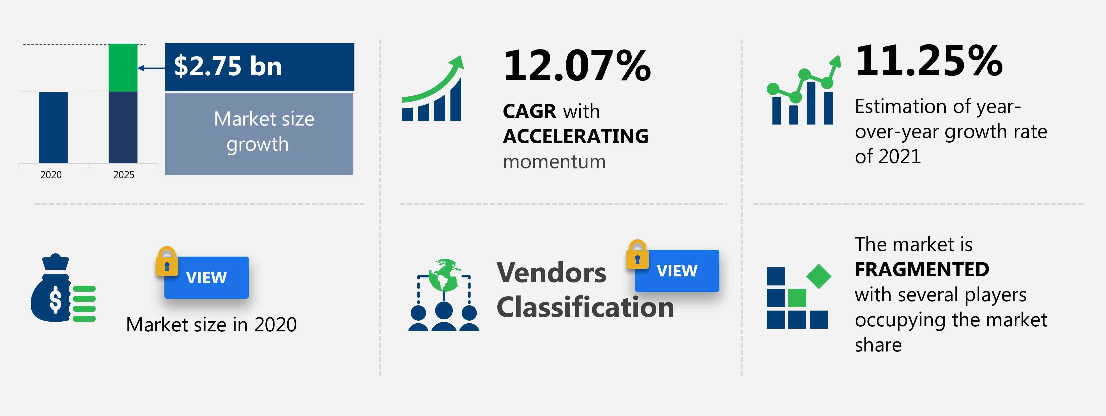
The epi wafer market share is expected to increase by USD 2.75 billion from 2020 to 2025, and the market’s growth momentum will accelerate at a CAGR of 12.07%.
This epi wafer market research report provides valuable insights on the post-COVID-19 impact on the market, which will help companies evaluate their business approaches. Furthermore, this report extensively covers epi wafer market segmentation by application (LED semiconductors, power semiconductors, MEMS-based devices, and others) and geography (North America, APAC, Europe, South America, and MEA). The epi wafer market report also offers information on several market vendors, including Applied Materials Inc., GlobalWafers Co. Ltd., II-VI Inc., IntelliEPI Inc., IQE Plc, Jenoptik AG, Nichia Corp., Shin-Etsu Chemical Co. Ltd., SHOWA DENKO K.K., and Xiamen Powerway Advanced Material Co. Ltd. among others.
What will the Epi Wafer Market Size be During the Forecast Period?
Download Report Sample to Unlock the Epi Wafer Market Size for the Forecast Period and Other Important Statistics
Epi Wafer Market: Key Drivers, Trends, and Challenges
Based on our research output, there has been a negative impact on the market growth during and post-COVID-19 era. The epitaxial deposition improves the performance of devices notably driving the epi wafer market growth, although factors such as the need for a thorough inspection of the epitaxial film surface may impede the market growth. Our research analysts have studied the historical data and deduced the key market drivers and the COVID-19 pandemic impact on the epi wafer industry. The holistic analysis of the drivers will help in deducing end goals and refining marketing strategies to gain a competitive edge.
Key Epi Wafer Market Driver
One of the key factors driving the Epi Wafer market is that epitaxial deposition improves the performance of devices. The deposition of an epitaxial layer on the wafer has grown since the year 2000. This is because the deposition helps enhance the performance of the devices such as transistors and ICs. The deposited layers are designed to have various compositional and electrical properties from the underlying wafer, which can be adjusted as per the requirements of devices such as transistors and ICs. The thorough inspection of the epitaxial layer makes it free of imperfections, reducing device failure and adding reliability at the time of fabrication. Further, this layer adds to the cost of device manufacturing; however, the overall benefits are much larger due to performance and functional improvements. The advantages of epitaxial wafers are they help in controlling the doping profile in a device structure that is formed by diffusion or ion implantation. Hence, such factors of epitaxial deposition will further drive the market growth.
Key Epi Wafer Market Trend
An increase in the number of fabless semiconductor companies and M&As is another factor supporting the Epi Wafer market growth in the forecast period. One of the main reasons for semiconductor companies going fabless is to minimize the overhead expenses in terms of operations and maintenance of foundries. Most semiconductor companies prefer to focus more on the design and development of their solutions. Therefore, they outsource their fabrication and other foundry-related activities to companies that provide such foundry solutions. Therefore, the ratio of foundries and fabless companies is 1:11 in the global semiconductor market. Furthermore, due to high costs, companies merge with or acquire other companies to increase their production facility and market share. For instance, in June 2021, Texas Instruments Inc. acquired all the assets related to the operations of a 300-mm semiconductor factory in Lehi, Utah, from Micron Technology, Inc. for a purchase price of $900 million. This, in turn, is increasing the consolidation in the semiconductor industry and the bargaining power of customers, which could lead to higher price negotiations, affecting the profit margins of the vendors.
Key Epi Wafer Market Challenge
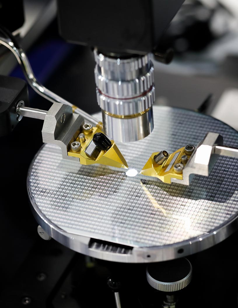
The need for a thorough inspection of the epitaxial film surface will be a major challenge for the Epi Wafer market during the forecast period. In an epitaxial deposition, the thin-layered film requires to be inspected at regular phases. The deposited layer is inspected thrice, first under bright lights, then using an optical microscope, and finally by a surface scanning laser defect counter. These devices help determine the presence of any impurities such as particles, spikes, scratches, pits, and haze. The bright light is used to reflect the surface of the epitaxial wafers; any deviation from a highly smooth and reflective surface is observed in this reflection. The optical microscope can magnify very small defects (75-200X) to view stacking faults and pyramidal defects. The laser scanner is used to double-check and quantify the remaining defects on the deposited epitaxial surface. This inspection process is complicated and time-consuming; hence, it affects the time-to-market of the end products such as IC chips. Therefore, this acts as a challenge, as manufacturers need to ensure timely delivery.
This epi wafer market analysis report also provides detailed information on other upcoming trends and challenges that will have a far-reaching effect on the market growth. The actionable insights on the trends and challenges will help companies evaluate and develop growth strategies for 2021-2025.
Parent Market Analysis
Technavio categorizes the global epi wafer market as a part of the global semiconductor equipment market within the global semiconductors and semiconductor equipment market. Our research report has extensively covered external factors influencing the parent market growth potential in the coming years, which will determine the levels of growth of the epi wafer market during the forecast period.
Who are the Major Epi Wafer Market Vendors?
The report analyzes the market’s competitive landscape and offers information on several market vendors, including:
- Applied Materials Inc.
- GlobalWafers Co. Ltd.
- II-VI Inc.
- IntelliEPI Inc.
- IQE Plc
- Jenoptik AG
- Nichia Corp.
- Shin-Etsu Chemical Co. Ltd.
- SHOWA DENKO K.K.
- Xiamen Powerway Advanced Material Co. Ltd.
This statistical study of the epi wafer market encompasses successful business strategies deployed by the key vendors. The epi wafer market is fragmented and the vendors are deploying growth strategies such as organic and inorganic growth strategies to compete in the market.
Product Insights and News
- Applied Materials Inc. - The company offers epi wafers under the brand name Centura Epi system.
To make the most of the opportunities and recover from the post-COVID-19 impact, market vendors should focus more on the growth prospects in the fast-growing segments, while maintaining their positions in the slow-growing segments.
The epi wafer market forecast report offers in-depth insights into key vendor profiles. The profiles include information on the production, sustainability, and prospects of the leading companies.
Epi Wafer Market Value Chain Analysis
Our report provides extensive information on the value chain analysis for the epi wafer market, which vendors can leverage to gain a competitive advantage during the forecast period. The end-to-end understanding of the value chain is essential in profit margin optimization and evaluation of business strategies. The data available in our value chain analysis segment can help vendors drive costs and enhance customer services during the forecast period.
The value chain of the global semiconductor equipment market includes the following core components:
- Inputs
- Inbound logistics
- Operations
- Outbound logistics
- Marketing and sales
- Service
- Support activities
- Innovation
The report has further elucidated other innovative approaches being followed by manufacturers to ensure a sustainable market presence.
Which are the Key Regions for Epi Wafer Market?
For more insights on the market share of various regions Request PDF Sample now!
75% of the market’s growth will originate from APAC during the forecast period. China, South Korea, and Japan are the key markets for the epi wafer market in APAC. Market growth in this region will be faster than the growth of the market in other regions.
The presence of nations with semiconductor manufacturing hubs such as South Korea and Japan will facilitate the epi wafer market growth in APAC over the forecast period. This market research report entails detailed information on the competitive intelligence, marketing gaps, and regional opportunities in store for vendors, which will assist in creating efficient business plans.
COVID Impact and Recovery Analysis
Manufacturing activities in APAC were adversely impacted in 2020 due to the COVID-19 pandemic. The imposition of stringent lockdowns and social distancing regulations forced many business owners to shut down their facilities temporarily. Therefore, with the onset of the COVID-19 pandemic, manufacturing was one of the severely hit sectors because of the challenges posed by supply and demand uncertainties. Besides, the shutdown of manufacturing bases for the electronic industry in China led to supply chain disruptions. However, industrial sectors such as automobile and manufacturing are expected to recover in the coming years, with the recommencing of business investment and consumer demand from 2021. This factor will positively impact the growth of the regional epi wafer market during the forecast period.
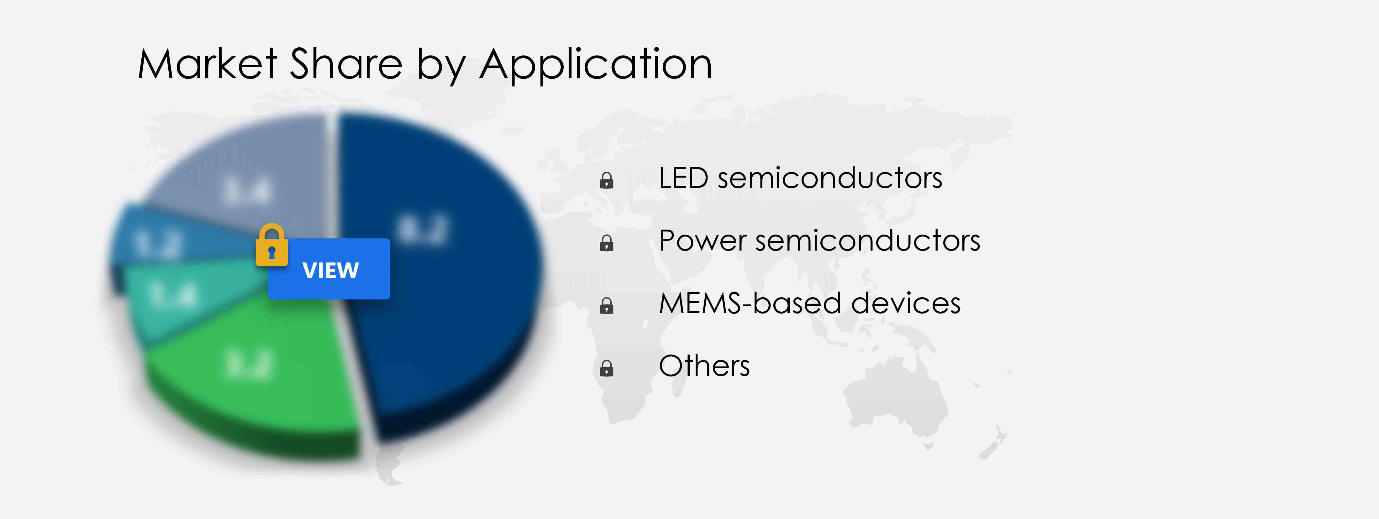
What are the Revenue-generating Application Segments in the Epi Wafer Market?
To gain further insights on the market contribution of various segments Request a PDF Sample
The epi wafer market share growth by the segments. LED semiconductors segment will be significant during the forecast period. LED lights are rapidly gaining traction among consumers due to their multiple benefits. LED lights are preferred over other lights, such as incandescent and compact fluorescent lamps (CFLs), due to their energy efficiency. Infrastructural development across the world and the emergence of the smart cities concept will foster immense growth in the LED market.
This report provides an accurate prediction of the contribution of all the segments to the growth of the epi wafer market size and actionable market insights on the post-COVID-19 impact on each segment.
|
Epi Wafer Market Scope |
|
|
Report Coverage |
Details |
|
Page number |
120 |
|
Base year |
2020 |
|
Forecast period |
2021-2025 |
|
Growth momentum & CAGR |
Accelerate at a CAGR of 12.07% |
|
Market growth 2021-2025 |
$ 2.75 billion |
|
Market structure |
Fragmented |
|
YoY growth (%) |
11.25 |
|
Regional analysis |
North America, APAC, Europe, South America, and MEA |
|
Performing market contribution |
APAC at 75% |
|
Key consumer countries |
China, South Korea (Republic of Korea), Japan, Taiwan, and the US |
|
Competitive landscape |
Leading companies, Competitive strategies, Consumer engagement scope |
|
Key companies profiled |
Applied Materials Inc., GlobalWafers Co. Ltd., II-VI Inc., IntelliEPI Inc., IQE Plc, Jenoptik AG, Nichia Corp., Shin-Etsu Chemical Co. Ltd., SHOWA DENKO K.K., and Xiamen Powerway Advanced Material Co. Ltd. |
|
Market dynamics |
Parent market analysis, Market growth inducers and obstacles, Fast-growing and slow-growing segment analysis, COVID 19 impact and recovery analysis and future consumer dynamics, Market condition analysis for the forecast period |
|
Customization purview |
If our report has not included the data that you are looking for, you can reach out to our analysts and get segments customized. |
What are the Key Data Covered in this Epi Wafer Market Report?
- CAGR of the market during the forecast period 2021-2025
- Detailed information on factors that will drive epi wafer market growth during the next five years
- Precise estimation of the epi wafer market size and its contribution to the parent market
- Accurate predictions on upcoming trends and changes in consumer behavior
- The growth of the epi wafer industry across North America, APAC, Europe, South America, and MEA
- A thorough analysis of the market’s competitive landscape and detailed information on vendors
- Comprehensive details of factors that will challenge the growth of epi wafer market vendors
We can help! Our analysts can customize this report to meet your requirements. Get in touch
 RIA -
RIA - 
