 Market by Type, End-user and Geography - Forecast and Analysis 2023-2027")

Enjoy complimentary customisation on priority with our Enterprise License!
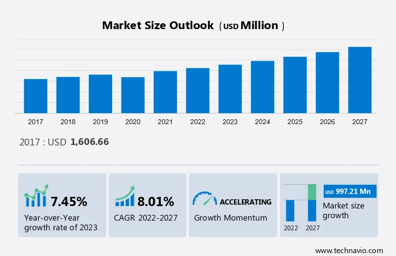
The global scanning electron microscope (SEMs) market size is estimated to grow by USD 997.21 million at a CAGR of 8.01% between 2022 and 2027.
Nanotechnology, rapidly advancing in science and technology, holds the potential to exert a positive influence on market expansion. The rapid need for product miniaturization, coupled with heightened consumer demands for compact yet robust devices at cost-effective rates, has propelled nanotechnology's popularity across diverse sectors. This innovative approach targets the manipulation of atoms, the tiniest particles, to harness their fundamental properties and attributes.
Leveraging nanoscience, technology constructs a comprehensive framework to realize this concept's potential. Given the myriad advantages spanning biomaterials, electronics, medicine, and microfabrication, substantial investments by both public and private domains in research and development underscore the enthusiasm to unlock nanotechnology's benefits. Notably, global leaders like the US and Japan allocate significant resources to nanotechnology initiatives. Projected to exhibit an impressive growth rate of approximately 18% during the forecast period, the escalating prominence of nanotechnology is poised to increase the demand for scanning electron microscopes (SEMs) which may have a positive impact on the scanning electron microscope (SEMs) market. This significant growth of nanotechnology will eventually enhance the demand for SEMs. Thus, increasing focus on nanotechnology is anticipated to drive market growth during the forecast period.
Technavio has segmented the market into Type, End-user and Geography
It also includes an in-depth analysis of drivers, trends, and challenges. Our report examines historic data from 2017 to 2021, besides analyzing the current market scenario.
To learn more about this report, Request Free Sample
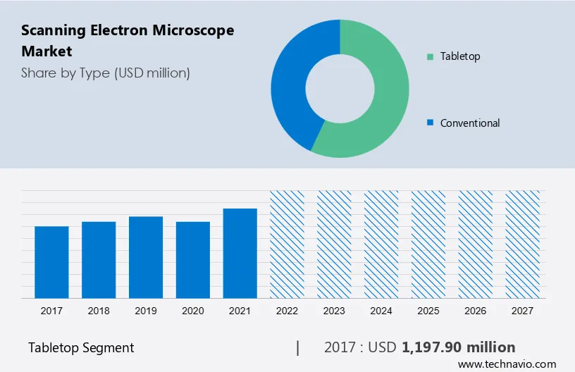
The market share growth by the tabletop segment will be significant during the forecast period. The tabletop category within the global scanning electron microscope market encompasses scanning electron microscope systems that are compact and portable, designed to be placed on tabletops. These units are smaller and lighter, allowing convenient installation, mobility, and relocation within laboratories and educational settings. This enhanced portability increases their accessibility and usability across different user groups. Furthermore, tabletop scanning electron microscopes are typically more cost-effective compared to conventional floor-standing models.
Get a glance at the market contribution of various segments View a PDF Sample
The tabletop segment was the largest segment and was valued at USD 1,197.90 million in 2017. Their affordability extends their availability to small research labs, educational institutions, and budget-restricted organizations, broadening the potential clientele. Designed for user-friendliness, tabletop scanning electron microscopes offer high-resolution imaging and efficient data capture despite their compact size. This segment facilitates access to electron microscopy for smaller labs and facilities without requiring extensive infrastructure adjustments. This inclusivity widens the user base for electron microscopy. Compared to larger systems, tabletop scanning electron microscopes generally entail simpler maintenance and servicing, minimizing operational downtime and expenses, thus enhancing their overall cost-efficiency. These factors are poised to propel the growth of the tabletop segment in the global scanning electron microscope market during the projected period.
In 2022, the semiconductors segment asserted its dominance in the worldwide scanning electron microscope market, a position it is projected to sustain in the forecasted period. A prime driving force behind this segment's growth is the escalating requirement for electronic device miniaturization from a diverse array of semiconductor and electronic component manufacturers. Semiconductors, encompassing silicon chips, find extensive application across an array of electronic devices, including computers. Nonetheless, sophisticated integrated circuits demand more advanced tools for functions like prototyping, development, examination, and failure analysis. The amalgamation of a scanning electron microscope with focus ion beam (FIB) technology presents a fitting solution, endowing remarkable precision alongside analytical capacities. The semiconductors sector within the global scanning electron microscope market is poised for expansion during the forecasted period.
The life science segment is playing a substantial role in propelling the expansion of the global scanning electron microscope market. Within this domain, scanning electron microscopes find diverse applications, assuming a pivotal role in cross-sectional precision imaging across various sectors, including microbiology, biology, botany, zoology, physiology, clinical pathology, toxicology, pharmacology, and biochemistry. By enabling the scrutiny of cellular structures and functions in three dimensions, as well as the ultrastructure of biomolecules and proteins, scanning electron microscopes have emerged as indispensable tools. As an emerging domain for advanced microscopes, the life sciences segment's growing adoption of scanning electron microscopes is anticipated to actuate the expansion of the global scanning electron microscope market during the forecast period.
For more insights about the market share of various regions View PDF Sample now!
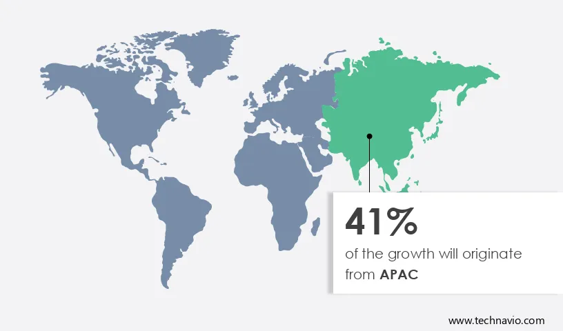
APAC is estimated to contribute 41% to the growth of the global market during the forecast period. Technavio’s analysts have elaborately explained the regional trends and drivers that will shape the scanning electron microscope (SEMs) market during the forecast period. In 2022, the APAC region held a commanding position in the global scanning electron microscope market, and this trend is poised to continue with the region exhibiting the swiftest growth rate in the future. As the primary producer and consumer of electronic devices, APAC plays a significant role in the scanning electron microscope market.
Furthermore, numerous semiconductor firms and consumer electronics manufacturers from beyond APAC have chosen to establish manufacturing facilities within the region or outsource their production processes to APAC-based entities. Another influential driver is India's Make in India campaign, which has drawn global manufacturers to establish production facilities in the country. This vibrant climate of technological advancement, particularly in nanotechnology, within APAC, is anticipated to fuel the demand for scanning electron microscopes, consequently propelling the growth of the regional scanning electron microscope market during the forecast period.
The emergence of the COVID-19 pandemic prompted an elevated utilization of scanning electron microscopes across a diverse range of end-users, including pharmaceuticals, hospitals, and research centers, during 2020. However, with the initiation of comprehensive vaccination campaigns orchestrated by various governments in the region during 2021, industrial activities in numerous sectors gradually resumed, thus rejuvenating the growth trajectory of the scanning electron microscope market. Notably, this region houses some of the globe's prominent semiconductor manufacturers, who are increasingly leveraging scanning electron microscopes for scrutinizing and characterizing semiconductor devices. These combined factors are poised to propel the expansion of the regional scanning electron microscope market during the forecast period.
Buy Now Full Report and Discover More
Companies are implementing various strategies, such as strategic alliances, partnerships, mergers and acquisitions, geographical expansion, and product/service launches, to enhance their presence in the market. The report also includes detailed analyses of the competitive landscape of the market and information about 20 market companies, including:
Advantest Corp - The company offers scanning electron microscopes such as MASK MVM SEM E3630, MASK MVM SEM E3640 and MASK DR SEM E5620.
Qualitative and quantitative analysis of companies has been conducted to help clients understand the wider business environment as well as the strengths and weaknesses of key market players. Data is qualitatively analyzed to categorize companies as pure play, category-focused, industry-focused, and diversified; it is quantitatively analyzed to categorize companies as dominant, leading, strong, tentative, and weak.
There are multiple factors influencing market growth. Our researchers analyzed the data with 2022 as the base year, along with the key drivers, trends, and challenges.
Increasing requirements for failure root cause analyses are notably driving the market growth. Technological advancements in the semiconductor and embedded system industries have elevated the manufacturing intricacy of ICs, sensors, and printed circuit boards (PCBs). This surge in complexity is driven by the pursuit of high-density products catering to sophisticated applications. Unlike optical microscopes, which face magnification limitations due to light wavelength, scanning electron microscopes (SEMs) offer a solution for detailed failure root cause analysis.
Moreover, this analytical approach, pivotal across sectors like automotive, manufacturing, research, and semiconductor, demands a precise view of the specific point requiring testing, where SEMs' superior image resolution capacity becomes invaluable. This growing recognition of SEMs' efficacy in failure root cause analyses is anticipated to be a driving force behind the expansion of the global scanning electron microscope market during the forecast period.
Miniaturization of electronic devices is an emerging trend shaping the market growth. The evolution of miniaturized electronic devices utilizing MEMSs and NEMSs is leading to lower power consumption in these devices. With the rise of compact personal electronic products, semiconductor foundries are striving to integrate diverse features, reduce semiconductor wafer sizes, and minimize IC power usage. Notably, the semiconductor sector has developed silicon wafers measuring 13.5 nm and 6 nm.
Moreover, NEMS technology is being employed by some firms for producing paper batteries, although it faces cost and commercialization constraints. Nevertheless, NEMS technology is anticipated to gain momentum during the forecast period, thereby augmenting the demand for scanning electron microscopes. These dynamics collectively contribute to the projected growth of the scanning electron microscope market during the forecast period.
Growing demand for TEMs is a major challenge hindering market growth. Transmission electron microscopes (TEMs) are instrumental in the examination of minute and slender specimens by transmitting electrons to generate projection images. Anticipated growth in demand for TEMs is expected to surpass that of scanning electron microscopes in the forecast period. TEMs serve as crucial tools for the analysis and characterization of a specimen's composition, structure, morphology, and features.
However, the submicron imagery they provide aids in comprehending material behaviour and finding utility across fields like geology, biology, and medical science. Given these manifold advantages, the expected period is likely to witness a notable surge in the demand for TEMs, potentially impacting the demand for scanning electron microscopes and may negatively influence the scanning electron microscope market growth. As a result, these dynamics could pose challenges to the growth of the global scanning electron microscope market during the forecast period.
Buy Now Full Report and Discover More
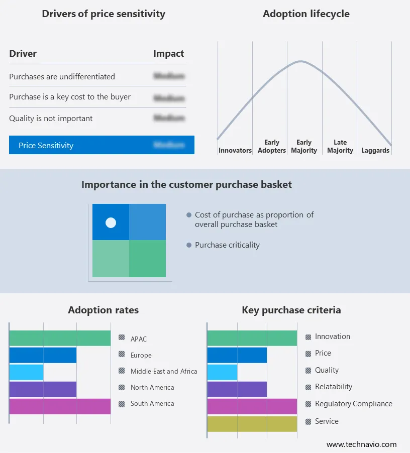
The market report includes the adoption lifecycle of the market, covering from the innovator’s stage to the laggard’s stage. It focuses on adoption rates in different regions based on penetration. Furthermore, the report also includes key purchase criteria and drivers of price sensitivity to help companies evaluate and develop their growth strategies.
Global Scanning Electron Microscope Market Customer Landscape
The scanning electron microscope market report forecasts market growth by revenue at global, regional & country levels and provides an analysis of the latest trends and growth opportunities from 2017 to 2027.
|
Scanning Electron Microscope Market Scope |
|
|
Report Coverage |
Details |
|
Page number |
172 |
|
Base year |
2022 |
|
Historic period |
2017-2021 |
|
Forecast period |
2023-2027 |
|
Growth momentum & CAGR |
Accelerate at a CAGR of 8.01% |
|
Market growth 2023-2027 |
USD 997.21 million |
|
Market structure |
Fragmented |
|
YoY growth 2022-2023(%) |
7.45 |
|
Regional analysis |
APAC, North America, Europe, South America, and Middle East and Africa |
|
Performing market contribution |
APAC at 41% |
|
Key countries |
US, China, Japan, South Korea, and Germany |
|
Competitive landscape |
Leading Vendors, Market Positioning of Vendors, Competitive Strategies, and Industry Risks |
|
Key companies profiled |
Advantest Corp., Agilent Technologies Inc., Bruker Corp., Carl Zeiss Stiftung, COXEM Co. Ltd., Danaher Corp., DELONG INSTRUMENTS AS, Hirox Co. Ltd., Hitachi Ltd., HOVERLABS, JEOL Ltd., Keysight Technologies Inc., Nikon Corp., Nion, Olympus Corp., Seiko Holdings Corp., Tescan Orsay Holding AS, Thermo Fisher Scientific Inc., Tokyo Instruments Inc., and Topcon Corp. |
|
Market dynamics |
Parent market analysis, Market growth inducers and obstacles, Fast-growing and slow-growing segment analysis, COVID-19 impact and recovery analysis and future consumer dynamics, Market condition analysis for the forecast period |
|
Customization purview |
If our report has not included the data that you are looking for, you can reach out to our analysts and get segments customized. |
View Sample PDF at your Fingertips
We can help! Our analysts can customize this market research report to meet your requirements. Get in touch
1 Executive Summary
2 Market Landscape
3 Market Sizing
4 Historic Market Size
5 Five Forces Analysis
6 Market Segmentation by Type
7 Market Segmentation by End-user
8 Customer Landscape
9 Geographic Landscape
10 Drivers, Challenges, and Trends
11 Vendor Landscape
12 Vendor Analysis
13 Appendix
Get lifetime access to our
Technavio Insights

Cookie Policy
The Site uses cookies to record users' preferences in relation to the functionality of accessibility. We, our Affiliates, and our Vendors may store and access cookies on a device, and process personal data including unique identifiers sent by a device, to personalise content, tailor, and report on advertising and to analyse our traffic. By clicking “I’m fine with this”, you are allowing the use of these cookies. Please refer to the help guide of your browser for further information on cookies, including how to disable them. Review our Privacy & Cookie Notice.