Scanning Electron Microscope Market Size 2024-2028
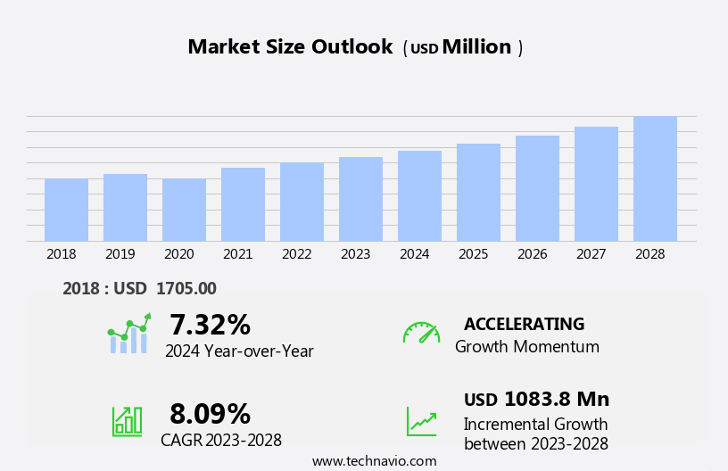
The scanning electron microscope (sems) market size is forecast to increase by USD 1.08 billion at a CAGR of 8.09% between 2023 and 2028.
- The Scanning Electron Microscope (SEM) market is experiencing significant growth driven by the increasing focus on nanotechnology and the increased demand for Large-Scale Variant SEMs (LVEMs). SEMs are essential tools in the field of materials science, electronics, and biology, enabling high-resolution imaging and analysis of surfaces at the nanoscale. The global adoption of SEMs is on the rise due to their ability to provide critical insights into the microstructure and composition of materials, which is crucial for research and development, quality control, and failure analysis. However, the high cost of SEMs remains a significant challenge for market growth. These sophisticated instruments require substantial investment and specialized expertise to operate effectively.
- Despite this, the potential benefits of SEM technology are compelling, and companies seeking to capitalize on market opportunities must navigate this challenge by exploring cost-effective solutions such as shared facilities, rental models, and collaborative partnerships. Additionally, ongoing advancements in SEM technology, including automation, software integration, and increased ease of use, are making these instruments more accessible and cost-effective for a wider range of applications and industries.
What will be the Size of the Scanning Electron Microscope (SEMS) Market during the forecast period?
- The Scanning Electron Microscope (SEM) market encompasses instruments utilized for high-resolution imaging and analysis of surface morphology, chemical composition, and nanoscale structures. This market plays a pivotal role in various sectors, including nanotechnology, semiconductor industry, electronics, materials science, biology, and medical devices. With advancements in detector technology and electron beam capabilities, SEMs offer magnification levels enabling the examination of minute details at the nanoscale. SEMs are instrumental in the semiconductor industry for the analysis of semiconductor wafers and the study of nanoscale materials. In materials science, SEMs facilitate the investigation of fractography and correlative microscopy techniques, complementing other methods such as light microscopy and Atomic Force Microscopy (AFM).
- In the realm of nanotechnology and electronics, SEMs enable the characterization of high-energy beam-induced damage and the analysis of complex nanostructures. Furthermore, in the medical field, SEMs contribute significantly to medical research by providing valuable insights into the surface characteristics of medical devices and biological samples. Overall, the SEM market continues to evolve, driven by the growing demand for intelligent technology and the need for increasingly precise analysis at the nanoscale.
How is this Scanning Electron Microscope (SEMS) Industry segmented?
The scanning electron microscope (sems) industry research report provides comprehensive data (region-wise segment analysis), with forecasts and estimates in "USD million" for the period 2024-2028, as well as historical data from 2018-2022 for the following segments.
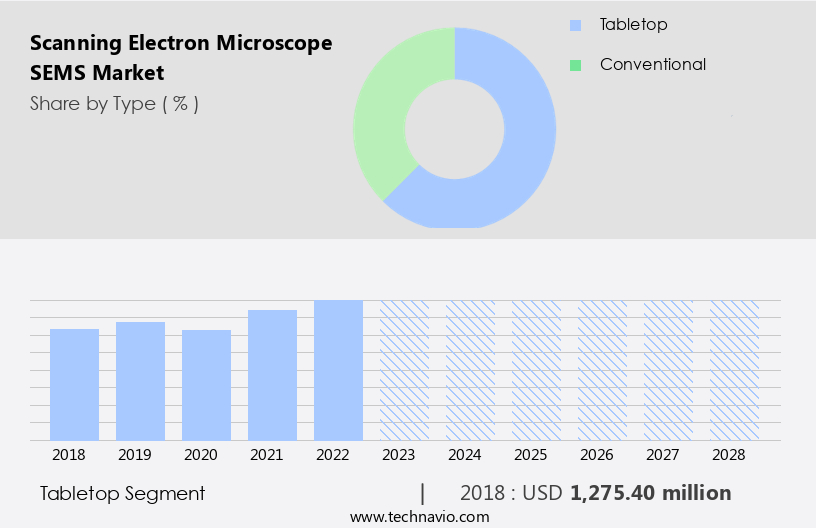
- Type
- Tabletop
- Conventional
- End-user
- Semiconductor
- Life sciences
- Material sciences
- Nanotechnology
- Application
- Quality Control Research and Development
- Failure Analysis
- Forensic Analysis
- Quality Control Research and Development
- Component
- Electron Gun
- Detectors
- Vacuum Systems
- Software
- Vacuum Systems
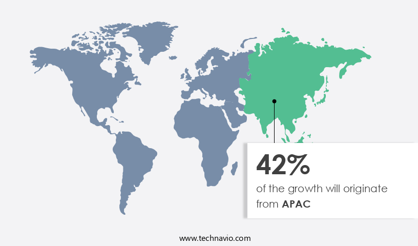
- Geography
- APAC
- China
- Japan
- South Korea
- North America
- US
- Canada
- Europe
- France
- Germany
- UK
- South America
- Middle East and Africa
- UAE
- Rest of World
- APAC
By Type Insights
The tabletop segment is estimated to witness significant growth during the forecast period.
The tabletop segment of the global scanning electron microscope (SEM) market caters to compact and portable SEM systems. These microscopes offer ease of installation, mobility, and flexibility for use in various laboratories and educational institutions. Their smaller size and reduced weight enable users to analyze nanoscale structures and surface morphology of materials in a more accessible and cost-effective manner. Tabletop SEMs are particularly beneficial for small research laboratories, educational institutions, and organizations with budget constraints. Designed with user-friendliness in mind, these microscopes feature intuitive interfaces and simplified operations, making them suitable for users with varying levels of experience in electron microscopy.
In nanotechnology, electronics, and materials science, SEMs play a crucial role in nanoscale imaging, chemical analysis, fractography, and failure analysis. They are extensively used in the semiconductor industry for material characterization, quality control, and transistor chip manufacturing. In the life sciences sector, SEMs are employed for imaging and analysis of nanofibers, nanotubes, temperature superconductors, and alloy strength. In medical research, they are used for chronic disease studies, clinical trials, and drug development. SEMs are also utilized in various industries, including aerospace, defense, environmental science, and forensics. They offer high-resolution imaging capabilities using electron beams, enabling the analysis of nanoscale structures and materials.
The market for SEMs is driven by the increasing demand for miniaturization and the need for advanced material characterization techniques. The adoption of intelligent technology and automated features in SEMs further enhances their capabilities and usability. Detector technology advancements, such as the development of high-energy beam detectors, have improved the magnification and imaging capabilities of SEMs. Additionally, the availability of correlative microscopy techniques, such as light microscopy and atomic force microscopy, has expanded the applications of SEMs. The market for SEMs is expected to continue growing due to the increasing demand for high-resolution imaging and analysis in various industries and research fields.
Get a glance at the market report of share of various segments Request Free Sample
The Tabletop segment was valued at USD 1.28 billion in 2018 and showed a gradual increase during the forecast period.
Regional Analysis
APAC is estimated to contribute 42% to the growth of the global market during the forecast period.Technavio's analysts have elaborately explained the regional trends and drivers that shape the market during the forecast period.
For more insights on the market size of various regions, Request Free Sample
The Scanning Electron Microscope (SEM) market is driven by the increasing demand for nanotechnology applications in various industries, including electronics, life sciences, and material sciences. With the miniaturization of transistor chips and the development of nanoscale materials such as nanofibers, nanotubes, and temperature superconductors, the need for high-resolution imaging and analysis techniques has become essential. SEMs provide surface morphology, chemical analysis, fractography, and failure analysis capabilities, making them indispensable tools for research institutions and industries. The market is segmented into nanotechnology applications, electronics, life sciences, material sciences, and others. Among these, nanotechnology applications are expected to dominate the market due to their extensive use in various industries, including drug development, material characterization, and correlative microscopy techniques.
The demand for SEMs is also high in industries such as aerospace, defense, environmental science, and forensics, where the analysis of nanoscale structures is crucial. The market is also influenced by factors such as the increasing use of intelligent technology and automated features in SEMs, user-friendly software, and the growing number of clinical trials for chronic diseases. However, high excise taxes and custom duties can pose challenges to the market growth. The SEM market includes various types of SEMs, such as high vacuum SEMs, low vacuum SEMs, cryo-SEMs, environmental SEMs, field emission SEMs, tabletop SEMs, dual-beam SEMs, and others.
The market is highly competitive, with several companies offering a range of SEM models catering to different industry requirements and budgets. In summary, the Scanning Electron Microscope market is expected to grow significantly due to the increasing demand for high-resolution imaging and analysis techniques in various industries. The market is segmented into nanotechnology applications, electronics, life sciences, material sciences, and others, with nanotechnology applications being the largest segment. The market is influenced by factors such as the increasing use of intelligent technology and automated features, user-friendly software, and the growing number of clinical trials. However, high excise taxes and custom duties can pose challenges to the market growth.
Market Dynamics
Our researchers analyzed the data with 2023 as the base year, along with the key drivers, trends, and challenges. A holistic analysis of drivers will help companies refine their marketing strategies to gain a competitive advantage.
What are the key market drivers leading to the rise in the adoption of Scanning Electron Microscope (SEMS) Industry?
- Increasing focus on nanotechnology is the key driver of the market.
- Nanotechnology, a rapidly advancing field of science and technology, is driving innovation across various industries due to the increasing demand for miniaturization and cost-effective, high-performance products. Nanotechnology enables manipulation of atoms, impacting their properties and features, which is crucial for the development of advanced materials and devices. Nanoparticles, a key component of nanotechnology, are integrated into numerous applications, from consumer goods such as clothing and cosmetics to industrial sectors like agriculture, automotive, and healthcare. Their usage spans from dental implants to tires, making them an indispensable part of our daily life.
- The global market for Scanning Electron Microscopes (SEMs), a critical tool in the nanotechnology industry, is expected to grow significantly due to the increasing research and development activities and the expanding applications of nanotechnology. SEMs provide high-resolution images of the surface of materials, enabling researchers to study the nanoscale properties and structures, thereby accelerating technological advancements.
What are the market trends shaping the Scanning Electron Microscope (SEMS) Industry?
- Increased demand for LVEMs is the upcoming market trend.
- Low-voltage electron microscopes (LVEMs) differ from traditional scanning electron microscopes (SEMs) in their use of a decelerating electron beam system and lower operating voltage of less than 25 kilovolts. This feature makes LVEMs more versatile as they can be used as tabletop or desktop devices, suitable for various laboratories. Compared to high-voltage electron microscopes (HVEMs), which operate at 100 kilovolts, LVEMs offer several advantages. They require less space, cost less, and provide high contrast with minimal damage to specimens. LVEMs are particularly beneficial for examining materials such as polymers, composite materials, pigments, minerals, cells, and membranes, as HVEMs can cause significant radiation accumulation and damage to these sensitive specimens.
- By utilizing LVEMs, laboratories can expand their capabilities while optimizing space and budget.
What challenges does the Scanning Electron Microscope (SEMS) Industry face during its growth?
- High cost of scanning electron microscope is a key challenge affecting the industry growth.
- Scanning Electron Microscopes (SEMs) are essential tools for various industries, providing high-resolution images of surfaces to facilitate material analysis. However, the high cost of these microscopes is a significant barrier to demand. SEMs can cost between USD100,000 and USD1,250,000, with non-analytical models selling for approximately USD700,000. Analytical SEMs typically range from USD400,000 to USD620,000. The price varies depending on the specifications and capabilities of each model. This high capital requirement limits the number of organizations that can afford to purchase SEMs, as many do not have the necessary budget.
- Despite the challenges, the demand for SEMs remains due to their crucial role in industries such as electronics, materials science, and biology. Organizations must carefully consider their budgets and the potential benefits of investing in an SEM before making a purchase.
Exclusive Customer Landscape
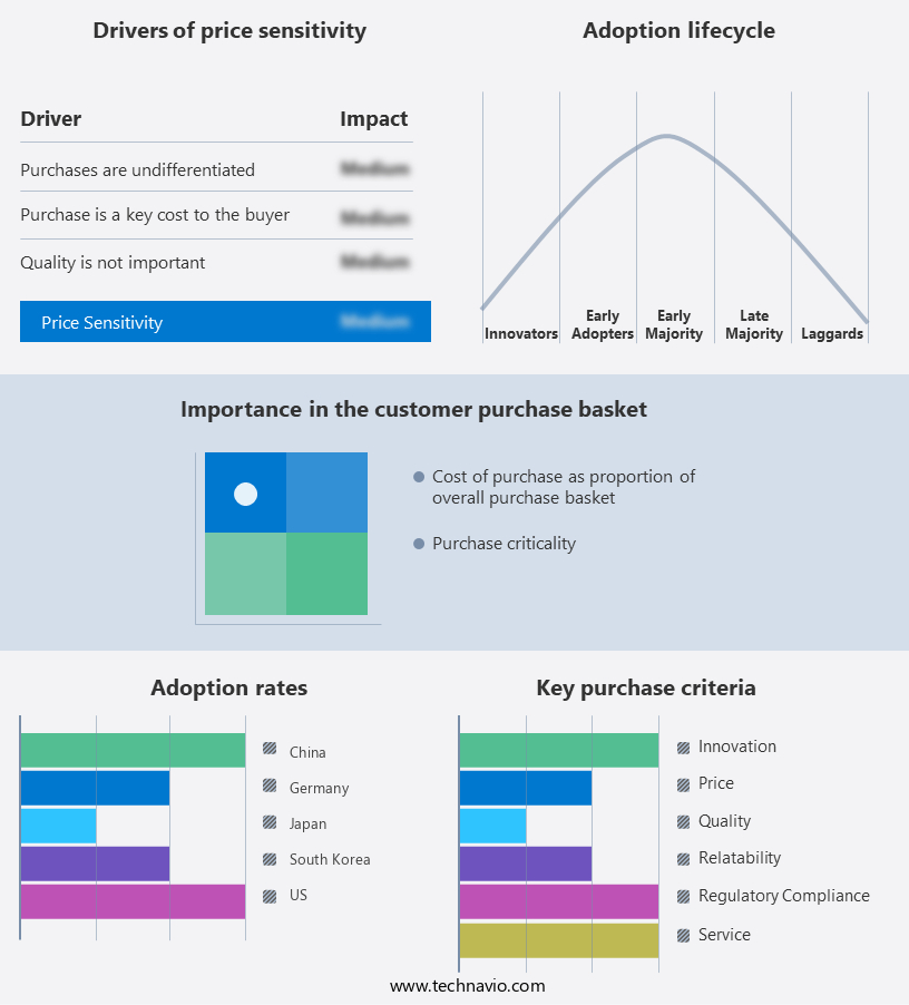
The scanning electron microscope (sems) market forecasting report includes the adoption lifecycle of the market, covering from the innovator's stage to the laggard's stage. It focuses on adoption rates in different regions based on penetration. Furthermore, the scanning electron microscope (sems) market report also includes key purchase criteria and drivers of price sensitivity to help companies evaluate and develop their market growth analysis strategies.
Customer Landscape
Key Companies & Market Insights
Companies are implementing various strategies, such as strategic alliances, scanning electron microscope (sems) market forecast, partnerships, mergers and acquisitions, geographical expansion, and product/service launches, to enhance their presence in the industry.
Advantest Corp. - The company provides advanced Scanning Electron Microscopes (SEMs) including the MASK MVM SEM E3630, MASK MVM SEM E3640, and MASK DR SEM E5620 models. These instruments deliver high-resolution imaging and analysis capabilities, enabling research and development teams to explore material structures at the nanoscale. With features such as advanced detectors, automated functions, and versatile sample preparation options, these SEMs empower users to gain valuable insights into various industries, from electronics to materials science.
The industry research and growth report includes detailed analyses of the competitive landscape of the market and information about key companies, including:
- Advantest Corp.
- Agilent Technologies Inc.
- Bruker Corp.
- Carl Zeiss Stiftung
- COXEM Co. Ltd.
- Danaher Corp.
- DELONG INSTRUMENTS AS
- Hirox Co. Ltd.
- Hitachi Ltd.
- HOVERLABS
- JEOL Ltd.
- Keysight Technologies Inc.
- Nikon Corp.
- Nion
- Olympus Corp.
- Seiko Holdings Corp.
- TESCAN GROUP
- Thermo Fisher Scientific Inc.
- Tokyo Instruments Inc.
- Topcon Corp.
Qualitative and quantitative analysis of companies has been conducted to help clients understand the wider business environment as well as the strengths and weaknesses of key industry players. Data is qualitatively analyzed to categorize companies as pure play, category-focused, industry-focused, and diversified; it is quantitatively analyzed to categorize companies as dominant, leading, strong, tentative, and weak.
Research Analyst Overview
The scanning electron microscope (SEM) market encompasses a broad range of applications in various industries, primarily driven by the advancements in nanotechnology and electronics. This market witnesses continuous growth due to the increasing demand for high-resolution imaging and analysis at the nanoscale. SEMs are essential tools in the field of nanoscale imaging, enabling the examination of surface morphology and chemical composition of samples with unparalleled detail. These microscopes utilize electron beams to scan the sample surface, generating high-resolution images and providing valuable information on the nanostructures and materials science behind various applications. The applications of SEMs span across numerous sectors, including electronics, life sciences, material sciences, and aerospace, among others.
In the electronics industry, SEMs play a crucial role in the miniaturization of transistor chips and the analysis of sample preparation processes. In the life sciences sector, SEMs are employed for material characterization and the study of nanofibers, nanotubes, and other nanomaterials, contributing significantly to medical research and drug development. The market dynamics for SEMs are influenced by several factors, including the demand for high-resolution imaging, the development of user-friendly software and automated features, and the increasing importance of quality control in various industries. Additionally, the growing trend towards intelligent technology and the integration of SEMs with other microscopy techniques, such as correlative microscopy and light microscopy, further expands the market potential.
Despite the numerous advantages of SEMs, the market faces challenges such as high excise taxes and custom duties, which can hinder the adoption of these microscopes in certain regions. Furthermore, the complexity and cost of SEMs can limit their accessibility to smaller research institutions and individual researchers. The SEM market is expected to continue its growth trajectory, driven by the increasing demand for nanoscale imaging and analysis across various industries. The ongoing advancements in detector technology, compact SEM models, and the development of high vacuum, low vacuum, cryo-SEMs, and other specialized SEM variants are further fueling the market growth.
In summary, the scanning electron microscope market represents a dynamic and growing industry, driven by the increasing demand for high-resolution nanoscale imaging and analysis across various sectors, including electronics, life sciences, material sciences, and aerospace. The market is influenced by several factors, including the development of user-friendly software and automated features, the importance of quality control, and the integration of SEMs with other microscopy techniques. Despite challenges such as high excise taxes and custom duties, the market is expected to continue its growth trajectory, driven by ongoing advancements in technology and the expanding applications of SEMs in various industries.
|
Market Scope |
|
|
Report Coverage |
Details |
|
Page number |
180 |
|
Base year |
2023 |
|
Historic period |
2018-2022 |
|
Forecast period |
2024-2028 |
|
Growth momentum & CAGR |
Accelerate at a CAGR of 8.09% |
|
Market growth 2024-2028 |
USD 1083.8 million |
|
Market structure |
Fragmented |
|
YoY growth 2023-2024(%) |
7.32 |
|
Key countries |
US, Canada, China, Japan, Germany, South Korea, UK, France, UAE, and Rest of World |
|
Competitive landscape |
Leading Companies, Market Positioning of Companies, Competitive Strategies, and Industry Risks |
What are the Key Data Covered in this Scanning Electron Microscope (SEMS) Market Research and Growth Report?
- CAGR of the Scanning Electron Microscope (SEMS) industry during the forecast period
- Detailed information on factors that will drive the growth and forecasting between 2024 and 2028
- Precise estimation of the size of the market and its contribution of the industry in focus to the parent market
- Accurate predictions about upcoming growth and trends and changes in consumer behaviour
- Growth of the market across APAC, North America, Europe, South America, and Middle East and Africa
- Thorough analysis of the market's competitive landscape and detailed information about companies
- Comprehensive analysis of factors that will challenge the scanning electron microscope (sems) market growth of industry companies
We can help! Our analysts can customize this scanning electron microscope (sems) market research report to meet your requirements.
 RIA -
RIA - 
