Enjoy complimentary customisation on priority with our Enterprise License!
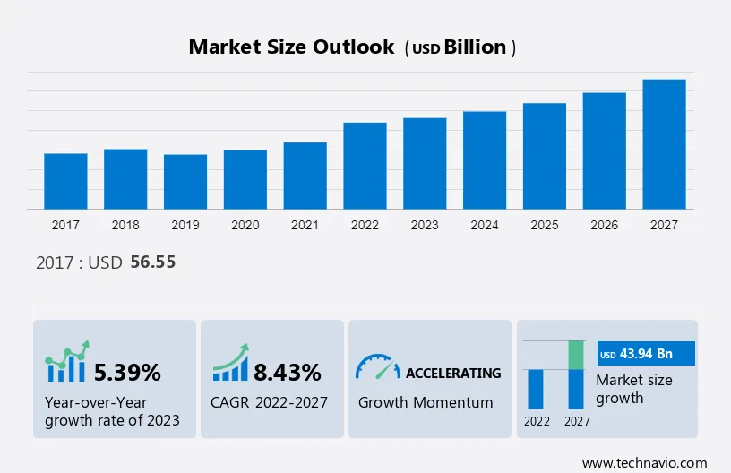
The wafer fab equipment (WFE) market size is estimated to grow by USD 43.94 billion at a CAGR of 8.43% between 2022 and 2027. The growth of the market depends on several factors, including Growing demand for consumer electronics, Increasing use of semiconductor chips in various industries, and Shift from traditional silicon-based technologies to advanced technologies like 5G, AI, IoT, and autonomous vehicles. Wafer fab equipment refers to the machinery and tools used in the fabrication process of ICs on semiconductor wafers. This equipment is vital in the production of ICs and includes a wide range of sophisticated tools such as photoresist coaters, photolithography systems, etching tools, deposition systems, ion implanters, metrology tools, and wafer handlers. These machines are used to deposit, etch, pattern, and test the various layers and components of the ICs during the manufacturing process.
It also includes an in-depth analysis of drivers, trends, and challenges. Furthermore, the report includes historic market data from 2017 to 2021.
To learn more about this report, View Report Sample
Growing demand for consumer electronics is the key driver for the growth of the market. With rapid advances in technology and the introduction of new features, consumers are constantly looking for the latest models with more powerful processors and more storage capacity. This has prompted smartphone manufacturers to invest heavily in upgrading their production facilities with advanced semiconductor wafer fab equipment. Wearable devices such as smartwatches, fitness trackers, and virtual reality headsets have grown in popularity in recent years. With the growing demand for wearable devices, the demand for advanced wafer fab equipment is expected to grow, presenting significant opportunities for the wafer fab equipment (WFE) market players.
Furthermore, the advent of IoT has led to the development of smart home appliances, connected cars, and industrial automation systems. These devices require rugged semiconductors that can handle complex tasks and communicate seamlessly with other devices. As a result, manufacturers of wafer fabrication equipment are seeing an increase in demand from industries beyond consumer electronics. Therefore, these factors are expected to drive the growth of the global market during the forecast period.
Technological advancements in the semiconductor industry are the primary trend shaping the growth of the market. A major technological breakthrough was the development of advanced lithography techniques. The lithography technique is an important step in semiconductor chip fabrication, as it involves transferring complex patterns onto thin silicon wafers. Another important advancement is the growing use of 3D microchip technology. 3D ICs stack multiple transistor layers on top of each other, delivering superior functionality and performance in a smaller footprint.
Moreover, the rise of IoT and connected devices has driven demand for low-power semiconductor chips. This need has led to the development of advanced manufacturing processes such as finned field-effect transistors (FinFETs) and nanowire transistors. These technologies allow for better control of power leakage, helping to create energy-efficient chips. Wafer fab equipment with advanced process control is required to fabricate these advanced transistors. Therefore, such factors will drive the growth of the market during the forecast period.
The high cost of equipment affects the growth of the market. The lithography machine is an example of high-cost equipment in the global market. These machines are essential in the manufacturing process as they are responsible for transferring the circuit samples onto the wafer surface. Advanced lithography machines, such as ultraviolet (EUV) lithography systems, can cost hundreds of millions of dollars. Due to the complexity and precision required to manufacture, the prices of these machines are high.
Furthermore, the etching process involves selectively removing specific layers from the semiconductor wafer to create patterns and structures. Advanced etching machines, such as deep reactive ion etching (DRIE) systems, are required to fabricate advanced semiconductor devices. Due to the complexity of the process and the requirement for precise control of the engraving parameters, these machines are expensive. Therefore, these factors are expected to impede the growth of the global market during the forecast period.
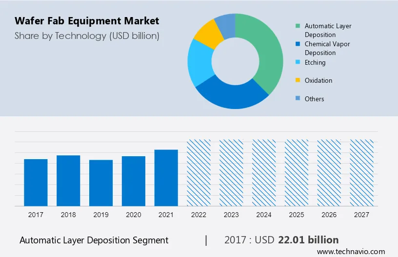
The market share growth by the automatic layer deposition segment will be significant during the forecast period. automatic layer dispositions have become popular in recent years, streamlining manufacturing processes and improving efficiency in the semiconductor industry. Automatic layer disposition also offers benefits beyond improving efficiency. By eliminating the need for manual labor, companies can reduce costs and reallocate resources to higher-value tasks.
Get a glance at the market contribution of various segments View Free PDF Sample
The automatic layer deposition showed a gradual increase in the market share of USD 22.01 billion in 2017 and continued to grow by 2021. An example is the use of machine learning (ML) algorithms to optimize layer layouts. By analyzing large amounts of data, these algorithms are able to identify patterns and trends that human traders might overlook. This allows the layer layout system to automatically make informed decisions about the best way to arrange the layers for optimal performance. In addition, the use of automated systems increases safety by minimizing worker exposure to potentially hazardous processes in the semiconductor industry. Hence, such features of automatic layer disposition may increase the adoption of the wafer fab equipment during the forecast period.
Foundries play an important role in the semiconductor industry by providing manufacturing services to companies that design and develop integrated circuits. The foundry segment in the global market is also benefiting from the growing trend of IC chip fabrication. Many companies, especially those focused on design and innovation, prefer to outsource the production process to foundries rather than invest in their own production facilities. This trend has led to increasing demand for semiconductor wafer fab equipment from foundries that are striving to provide competitive and efficient fabrication services to a wide variety of customers. To meet the needs of the foundry segment, market players are continuously developing and introducing innovative solutions. This equipment enables foundries to achieve the desired quality, output, and productivity in their production processes. Hence, these factors are expected to increase the demand for wafer fab equipment in the foundry segment, which will drive the growth of the market during the forecast period.
For more insights on the market share of various regions Download PDF Sample now!
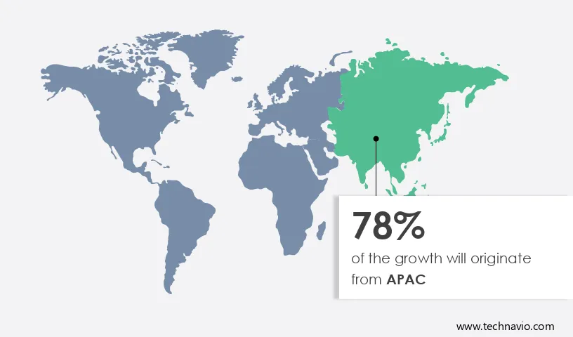
APAC is estimated to contribute 78% to the growth of the global market during the forecast period. Technavio’s analysts have elaborately explained the regional trends and drivers that shape the market during the forecast period. With factors such as a thriving semiconductor industry, technological advancements, and growing demand for electronic devices, APAC has become a hub for wafers fabrication equipment. One of the key factors contributing to the growth of the market in the region is the presence of major semiconductor manufacturers in the region.
In addition, government initiatives to promote and support the semiconductor industry in the APAC region also play an important role in the growth of the global market. The availability of skilled labor at a lower cost than in other regions such as North America and Europe, coupled with the presence of a strong supply chain network, further fueled the growth of the market in APAC. Hence, these factors will drive the growth of the regional market during the forecast period.
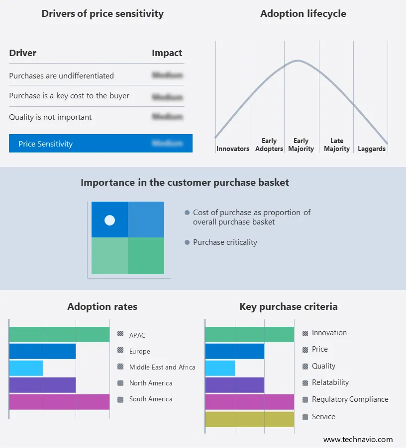
The Market report includes the adoption lifecycle of the market, covering from the innovator’s stage to the laggard’s stage. It focuses on adoption rates in different regions based on penetration. Furthermore, the report also includes key purchase criteria and drivers of price sensitivity to help companies evaluate and develop their growth strategies.
Global Wafer Fab Equipment Market Customer Landscape
Companies are implementing various strategies, such as strategic alliances, partnerships, mergers and acquisitions, geographical expansion, and product/service launches, to enhance their presence in the market.
The research report also includes detailed analyses of the competitive landscape of the market and information about 20 market companies, including:
Qualitative and quantitative analysis of companies has been conducted to help clients understand the wider business environment as well as the strengths and weaknesses of key market players. Data is qualitatively analyzed to categorize companies as pure play, category-focused, industry-focused, and diversified; it is quantitatively analyzed to categorize companies as dominant, leading, strong, tentative, and weak.
The market report forecasts market growth by revenue at global, regional & country levels and provides an analysis of the market growth and trends opportunities from 2017 to 2027.
The Market is influenced by various factors, including disposable income and population growth, which drive demand for consumer appliances and semiconductor Fab Equipment. These devices rely on advanced electrical circuits produced using wafer fab equipment. The telecommunications sector is a key consumer of wafer fab equipment, requiring high-performance components for their infrastructure. To meet this demand, manufacturers focus on creating an all-inclusive environment for semiconductor production.
Market research in this sector involves both secondary research and primary interviews, along with in-house expert reviews. Analysts also consider social, political, and economic factors, conducting Porter's Five Forces analysis to assess buyers' and suppliers' bargaining power, the threat of new entrants, the threat of substitutes, and the degree of competition. System integrators play a crucial role in the wafer fab equipment market, facilitating the seamless integration of components into larger systems. As technology advances, the market continues to evolve, driving innovation in semiconductor manufacturing.
|
Wafer Fab Equipment Market Scope |
|
|
Report Coverage |
Details |
|
Page number |
167 |
|
Base year |
2022 |
|
Historic period |
2017-2021 |
|
Forecast period |
2023-2027 |
|
Growth momentum & CAGR |
Accelerate at a CAGR of 8.43% |
|
Market growth 2023-2027 |
USD 43.94 billion |
|
Market structure |
Fragmented |
|
YoY growth 2022-2023(%) |
5.39 |
|
Regional analysis |
APAC, North America, Europe, Middle East and Africa, and South America |
|
Performing market contribution |
APAC at 78% |
|
Key countries |
US, Taiwan, China, South Korea, and Japan |
|
Competitive landscape |
Leading Companies, Market Positioning of Companies, Competitive Strategies, and Industry Risks |
|
Key companies profiled |
ASML, AIXTRON SE, Applied Materials Inc., ASM International NV, ASMPT Ltd., Baxter International Inc., EV Group, FormFactor Inc., Hitachi Ltd., HORIBA Ltd., KLA Corp., KOKUSAI ELECTRIC CORP., Lam Research Corp., Nikon Corp., PLASMA THERM, Taiwan Semiconductor Manufacturing Co. Ltd., Teradyne Inc., Tokyo Electron Ltd., Screen Holdings Co. Ltd., and Hanmi Semiconductor Co. Ltd. |
|
Market dynamics |
Parent market analysis, Market forecasting, Market growth inducers and obstacles, Fast-growing and slow-growing segment analysis, COVID-19 impact and recovery analysis and future consumer dynamics, and Market condition analysis for the market forecast period. |
|
Customization purview |
If our market research report has not included the data you are looking for, you can reach out to our analysts and get customized segments. |
We can help! Our analysts can customize this market research report to meet your requirements.
1 Executive Summary
2 Market Landscape
3 Market Sizing
4 Historic Market Size
5 Five Forces Analysis
6 Market Segmentation by Technology
7 Market Segmentation by End-user
8 Customer Landscape
9 Geographic Landscape
10 Drivers, Challenges, and Trends
11 Vendor Landscape
12 Vendor Analysis
13 Appendix
Get lifetime access to our
Technavio Insights
 Market Analysis APAC, North America, Europe, Middle East and Africa, South America - US, Taiwan, China, South Korea, Japan - Size and Forecast 2023-2027")

