Wafer Fab Equipment (WFE) Market Size 2025-2029
The wafer fab equipment (wfe) market size is forecast to increase by USD 34.7 billion, at a CAGR of 6.2% between 2024 and 2029.
- The market is driven by the surging demand for consumer electronics, fueling the need for advanced semiconductor technologies. The semiconductor industry's continuous technological innovations further bolster this market's growth. However, the high cost of wafer fab equipment poses a significant challenge for market participants. Companies must navigate this obstacle by implementing cost-effective production strategies or seeking partnerships to share the financial burden.
- This dynamic market landscape requires strategic planning and operational agility from WFE manufacturers and end-users alike. To capitalize on opportunities and mitigate challenges, industry players must stay abreast of the latest technological advancements and market trends while maintaining a competitive edge through cost optimization and strategic collaborations.
What will be the Size of the Wafer Fab Equipment (WFE) Market during the forecast period?

Explore in-depth regional segment analysis with market size data - historical 2019-2023 and forecasts 2025-2029 - in the full report.
Request Free Sample
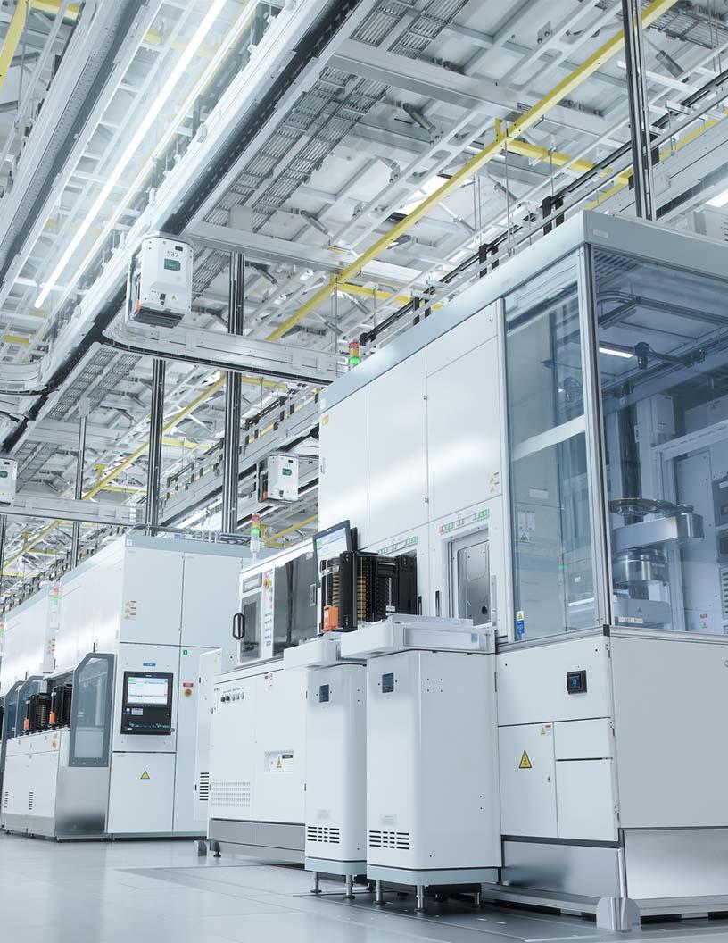
The market is characterized by continuous evolution and dynamic market activities. Plasma etching and dry etching technologies play crucial roles in shaping device performance by precisely removing material from silicon wafers. DUV lithography and EUV lithography are essential for pattern definition, with immersion lithography continuing to dominate the industry. Wafer cleaning and handling processes ensure wafer quality, while thin film deposition techniques enhance chip density and transistor performance. Process development and integration are ongoing priorities, with advanced node manufacturing pushing scaling limits. Wafer tracking and capacity planning are vital for optimizing production and minimizing operating expenses.
Smart manufacturing and factory automation are transforming semiconductor manufacturing, enabling real-time data analytics and predictive maintenance. Wafer lifetime, wafer diameter, and wafer thickness are essential factors in cost of ownership calculations. Preventive maintenance and spare parts management are critical for maintaining equipment reliability and minimizing downtime. Wafer testing, defect density, and performance metrics are integral to yield optimization, ensuring high-quality substrate materials and minimizing power consumption. Epitaxial wafers and wafer bonding are essential steps in the fabrication process. Lithography tools and wafer dicers are indispensable components of the WFE ecosystem. Air filtration and particle control are essential for maintaining cleanroom technology and ensuring product quality.
The technology roadmap for WFE is ever-evolving, with ongoing advancements in process control, yield optimization, and technology integration driving productivity improvement and cost reduction. Moore's Law continues to shape the industry, pushing the boundaries of what is possible in semiconductor manufacturing.
How is this Wafer Fab Equipment (WFE) Industry segmented?
The wafer fab equipment (wfe) industry research report provides comprehensive data (region-wise segment analysis), with forecasts and estimates in "USD billion" for the period 2025-2029, as well as historical data from 2019-2023 for the following segments.
- Technology
- Automatic layer deposition
- Chemical vapor diposition
- Etching
- Oxidation
- Others
- End-user
- Foundry
- Memory
- Integrated device manufacturer
- Capacity
- 300 mm wafer size
- 200 mm wafer size
- 150 mm wafer size
- Product Specification
- Node size between 14nm and 28nm
- Node size between 7nm and 14nm
- Node size more than 28nm
- Node size between 5nm and 7nm
- Node size below 5nm
- Geography
- North America
- US
- Canada
- Europe
- France
- Germany
- UK
- APAC
- China
- India
- Japan
- South Korea
- Taiwan
- Rest of World (ROW)
- North America
By Technology Insights
The automatic layer deposition segment is estimated to witness significant growth during the forecast period.
In the semiconductor manufacturing sector, advancements in technology have led to the widespread adoption of automation and data-driven solutions. For instance, automatic layer deposition (ALD) using robotic systems is transforming wafer fab facilities. These systems autonomously arrange and stack multiple layers of silicon wafers, thereby reducing human error and increasing production speed. Moreover, machine learning (ML) algorithms are being employed to optimize layer deposition processes. By analyzing vast data sets, these algorithms identify patterns and trends, enhancing process efficiency and yield. Wafer quality is a critical factor in semiconductor manufacturing. Wafer diameter, thickness, and defect density are essential performance metrics.
Wafer testing, cleaning, handling, and bonding are integral parts of the fabrication process. Immersion lithography, plasma etching, and dry etching are essential lithography tools. Advanced nodes, such as EUV lithography, push the boundaries of technology roadmaps, enabling higher transistor densities and chip complexity. Smart manufacturing and production optimization are essential for minimizing operating expenses and maximizing productivity. Capacity planning, technology integration, and process control are crucial for managing the complex semiconductor manufacturing process. Factory automation, tool maintenance, and spare parts management are vital for maintaining a consistent production flow. Cost of ownership, wafer lifetime, and equipment calibration are essential considerations for semiconductor manufacturers.
Substrate materials, such as epitaxial wafers, play a significant role in determining wafer quality and performance. Moore's Law continues to drive the need for constant innovation and productivity improvement. Data analytics and process simulation are essential for optimizing semiconductor manufacturing processes. Preventive maintenance, equipment qualification, and cleanroom technology are crucial for maintaining a reliable and efficient manufacturing environment. Reliability testing, air filtration, and power consumption are essential factors in ensuring the long-term performance and reliability of semiconductor devices. In conclusion, the semiconductor manufacturing industry is undergoing a transformation, driven by automation, data-driven solutions, and technological innovation. The integration of advanced tools and processes, such as ALD, ML algorithms, and EUV lithography, is essential for pushing the boundaries of semiconductor technology and meeting the demands of the ever-evolving market.

The Automatic layer deposition segment was valued at USD 21.60 billion in 2019 and showed a gradual increase during the forecast period.
Regional Analysis
APAC is estimated to contribute 77% to the growth of the global market during the forecast period.Technavio’s analysts have elaborately explained the regional trends and drivers that shape the market during the forecast period.

In The market, APAC holds a significant role due to its robust semiconductor industry, technological advancements, and increasing demand for electronic devices. Major semiconductor manufacturers, including Taiwan Semiconductor Manufacturing Co (TSMC), Samsung Electronics Co. Ltd (Samsung), and SK Hynix (SK Hynix), have established advanced fabrication facilities in APAC, necessitating sophisticated wafer fab equipment. These companies prioritize yield enhancement, wafer quality, and chip density to maintain their competitive edge. Automated material handling, wafer testing, particle control, and smart manufacturing are essential for optimizing production and ensuring wafer tracking. Immersion lithography, wet etching, and advanced node technologies facilitate process integration and enable scaling limits.
Tool maintenance, factory automation, and process control are crucial for semiconductor manufacturing, while capacity planning and cost of ownership are essential considerations. Substrate materials, wafer lifetime, and process optimization are integral to wafer fabrication, which includes wafer bonding, plasma etching, and duv lithography. Wafer cleaning, handling, and dry etching are necessary for device performance. Thin film deposition and equipment calibration are essential for process development. Defect density and performance metrics, including wafer thickness and equipment qualification, are vital for preventive maintenance and cleanroom technology. Moore's law continues to drive productivity improvement, and euv lithography is poised to revolutionize the industry.
Market Dynamics
Our researchers analyzed the data with 2024 as the base year, along with the key drivers, trends, and challenges. A holistic analysis of drivers will help companies refine their marketing strategies to gain a competitive advantage.
What are the key market drivers leading to the rise in the adoption of Wafer Fab Equipment (WFE) Industry?
- The expanding consumer electronics market is primarily fueled by increasing demand from consumers.
- The market is experiencing substantial growth due to the increasing demand from the consumer electronics sector. Advanced wafer fab equipment is essential for manufacturing high-performance components, such as epitaxial wafers and transistors, which are integral to the production of smartphones, tablets, and laptops. These devices have become indispensable in modern life, leading to a constant quest for innovation and improved functionality. Manufacturers are investing heavily in upgrading their production facilities with advanced WFE to meet consumer demands for more powerful processors and higher storage capacities. Moore's Law, which predicts the exponential increase in transistor density on integrated circuits, continues to drive the need for productivity improvement and process integration in wafer fabrication.
- Lithography tools, wafer dicing equipment, and power consumption management systems are crucial components of the WFE market. Reliability testing, air filtration, and equipment calibration are also essential for maintaining the high standards required in semiconductor manufacturing. The focus on process simulation and wafer bonding ensures the production of high-quality, consistent components. Capital expenditure on WFE is a significant investment for semiconductor manufacturers, and the market is expected to continue growing as the demand for advanced electronics increases. The importance of WFE in the semiconductor industry cannot be overstated, as it enables the production of the technology that powers our daily lives.
What are the market trends shaping the Wafer Fab Equipment (WFE) Industry?
- The semiconductor industry is currently experiencing significant technological advancements, which is a notable market trend. Advancements in semiconductor technology are driving innovation and growth within this industry.
- The market has experienced notable growth due to technological advancements in the semiconductor industry. These innovations have led to the production of smaller, faster, and more efficient semiconductor chips. A significant technological development is the enhancement of lithography techniques. Lithography is an essential process in semiconductor chip manufacturing, which involves transferring complex patterns onto silicon wafers. Traditional optical lithography methods have limitations in terms of resolution and precision. However, the introduction of advanced techniques like EUV lithography enables higher resolution and more precise patterning. Moreover, other processes such as plasma etching, thin film deposition, wafer cleaning, and wafer handling are crucial in semiconductor manufacturing.
- These processes ensure device performance by controlling defect density and maintaining wafer thickness. Dry etching, for instance, is a critical process used to remove unwanted material from wafers, while cleanroom technology ensures a clean environment to prevent contamination. Process development is another essential aspect of the WFE market, as it involves continuous improvement to meet the evolving demands of semiconductor manufacturing. Equipment qualification and preventive maintenance are also essential to ensure the longevity and efficiency of WFE. In conclusion, the WFE market's growth is driven by the semiconductor industry's technological advancements and the need for higher performance and efficiency in semiconductor chips.
What challenges does the Wafer Fab Equipment (WFE) Industry face during its growth?
- The exorbitant cost of wafer fabrication equipment poses a significant challenge to the expansion and growth of the semiconductor industry.
- The market experiences continuous growth due to the increasing demand for advanced semiconductor technologies. Wafer quality and chip density are key factors driving this market, necessitating the use of sophisticated equipment for defect inspection, particle control, and wafer testing. Automated material handling systems and smart manufacturing solutions further enhance yield and optimize production. Lithography machines, a significant investment in WFE, are essential for transferring circuit patterns onto silicon wafers. Their high cost contributes to the overall expense of semiconductor manufacturing.
- Wafer tracking and technology roadmap integration are crucial for maintaining process control and addressing scaling limits. In conclusion, the global WFE market's dynamics revolve around the need for high-performance, cost-effective equipment to meet the evolving demands of the semiconductor industry.
Exclusive Customer Landscape
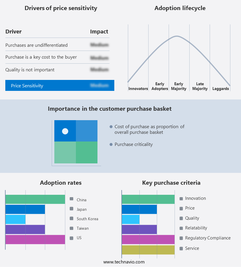
The wafer fab equipment (wfe) market forecasting report includes the adoption lifecycle of the market, covering from the innovator’s stage to the laggard’s stage. It focuses on adoption rates in different regions based on penetration. Furthermore, the wafer fab equipment (wfe) market report also includes key purchase criteria and drivers of price sensitivity to help companies evaluate and develop their market growth analysis strategies.
Customer Landscape
Key Companies & Market Insights
Companies are implementing various strategies, such as strategic alliances, wafer fab equipment (wfe) market forecast, partnerships, mergers and acquisitions, geographical expansion, and product/service launches, to enhance their presence in the industry.
AIXTRON SE - This company specializes in the production of advanced wafer fab equipment, specifically focusing on deposition systems designed for compound semiconductors. Our offerings facilitate the manufacturing process for these materials, enhancing efficiency and productivity. By utilizing cutting-edge technology, we ensure the highest quality and reliability for our clients in the global semiconductor industry. Our deposition systems cater to various compound semiconductor applications, including power electronics, radio frequency (RF) components, and optoelectronics. Our commitment to innovation and excellence drives us to continually push the boundaries of what's possible in semiconductor manufacturing.
The industry research and growth report includes detailed analyses of the competitive landscape of the market and information about key companies, including:
- AIXTRON SE
- Applied Materials Inc.
- ASM International NV
- ASML
- ASMPT Ltd.
- Baxter International Inc.
- EV Group
- FormFactor Inc.
- Hanmi Semiconductor Co. Ltd.
- Hitachi Ltd.
- HORIBA Ltd.
- KLA Corp.
- KOKUSAI ELECTRIC CORP
- Lam Research Corp.
- Nikon Corp.
- PLASMA THERM
- Screen Holdings Co. Ltd
- Taiwan Semiconductor Manufacturing Co. Ltd.
- Teradyne Inc.
- Tokyo Electron Ltd.
Qualitative and quantitative analysis of companies has been conducted to help clients understand the wider business environment as well as the strengths and weaknesses of key industry players. Data is qualitatively analyzed to categorize companies as pure play, category-focused, industry-focused, and diversified; it is quantitatively analyzed to categorize companies as dominant, leading, strong, tentative, and weak.
Recent Development and News in Wafer Fab Equipment (WFE) Market
- In January 2024, ASML Holding NV, a leading provider of photolithography equipment for the semiconductor industry, announced the launch of its new EUV lithography system, the NXT:3400Gi. This state-of-the-art equipment promises to significantly improve manufacturing efficiency and reduce costs for chipmakers (ASML Press Release, 2024).
- In March 2024, Intel Corporation and Taiwan Semiconductor Manufacturing Company (TSMC) announced a strategic collaboration to co-develop advanced semiconductor technologies. This partnership aims to accelerate the development and production of next-generation chips, addressing the increasing demand for advanced technology in various industries (Intel Press Release, 2024).
- In October 2024, Lam Research Corporation completed the acquisition of KLA Corporation's Wafer Fab Services business. This acquisition expanded Lam Research's services portfolio, enabling the company to offer a comprehensive suite of solutions to its customers, from wafer fabrication to final test and packaging (Lam Research Press Release, 2024).
- In May 2025, the South Korean government announced a USD45 billion investment in the semiconductor industry over the next five years. This significant investment is aimed at expanding the country's manufacturing capacity and strengthening its position as a global leader in the Wafer Fab Equipment market (Yonhap News Agency, 2025).
Research Analyst Overview
- The market is characterized by continuous innovation and advancements in technology. Key technologies shaping the industry include Data Visualization, Overlay Measurement, Artificial Intelligence (AI), and Nanoimprint Lithography. AI and Machine Learning (ML) are revolutionizing process control systems, enabling Predictive Modeling and Yield Management. Direct Write and Maskless Lithography are transforming fabrication processes, with Extreme Ultraviolet (EUV) and Deep Ultraviolet (DUV) gaining traction. Wafer Inspection and Test Equipment are essential for maintaining quality and efficiency. Wafer probing ensures accurate measurement and analysis of semiconductor devices.
- Process control systems employ advanced technologies like Electron Beam Lithography to ensure precision and consistency. Overlay measurement plays a crucial role in aligning layers during manufacturing, while Die Sort and Wafer Steppers facilitate the production of high-performance chips. These technologies contribute to the dynamic and evolving WFE market landscape.
Dive into Technavio’s robust research methodology, blending expert interviews, extensive data synthesis, and validated models for unparalleled Wafer Fab Equipment (WFE) Market insights. See full methodology.
|
Market Scope |
|
|
Report Coverage |
Details |
|
Page number |
232 |
|
Base year |
2024 |
|
Historic period |
2019-2023 |
|
Forecast period |
2025-2029 |
|
Growth momentum & CAGR |
Accelerate at a CAGR of 6.2% |
|
Market growth 2025-2029 |
USD 34.7 billion |
|
Market structure |
Fragmented |
|
YoY growth 2024-2025(%) |
5.8 |
|
Key countries |
China, South Korea, Japan, US, Taiwan, India, Canada, Germany, France, and UK |
|
Competitive landscape |
Leading Companies, Market Positioning of Companies, Competitive Strategies, and Industry Risks |
What are the Key Data Covered in this Wafer Fab Equipment (WFE) Market Research and Growth Report?
- CAGR of the Wafer Fab Equipment (WFE) industry during the forecast period
- Detailed information on factors that will drive the growth and forecasting between 2025 and 2029
- Precise estimation of the size of the market and its contribution of the industry in focus to the parent market
- Accurate predictions about upcoming growth and trends and changes in consumer behaviour
- Growth of the market across APAC, North America, Europe, Middle East and Africa, and South America
- Thorough analysis of the market’s competitive landscape and detailed information about companies
- Comprehensive analysis of factors that will challenge the wafer fab equipment (wfe) market growth of industry companies
We can help! Our analysts can customize this wafer fab equipment (wfe) market research report to meet your requirements.
 RIA -
RIA - 
