Semiconductor Wafer Inspection Equipment Market Size 2026-2030
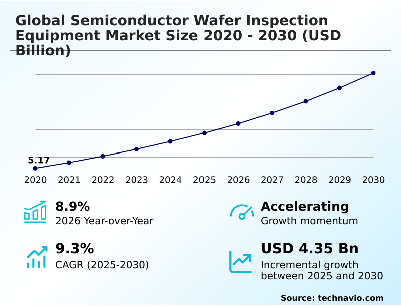
The semiconductor wafer inspection equipment market size is valued to increase by USD 4.35 billion, at a CAGR of 9.3% from 2025 to 2030. Proliferation of advanced process nodes and complex chip architectures will drive the semiconductor wafer inspection equipment market.
Major Market Trends & Insights
- APAC dominated the market and accounted for a 74.9% growth during the forecast period.
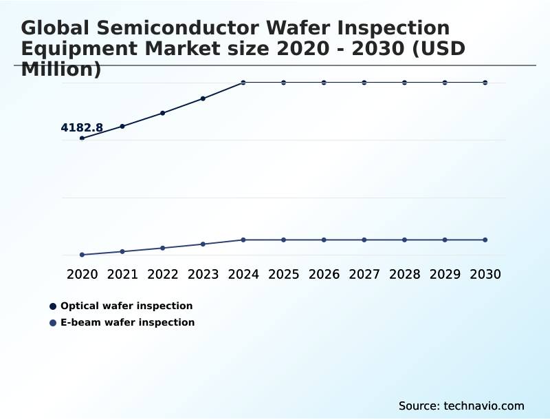
- By Type - Optical wafer inspection segment was valued at USD 5.72 billion in 2024
- By Application - Front-end process inspection segment accounted for the largest market revenue share in 2024
Market Size & Forecast
- Market Opportunities: USD 6.91 billion
- Market Future Opportunities: USD 4.35 billion
- CAGR from 2025 to 2030 : 9.3%
Market Summary
- The semiconductor wafer inspection equipment market is foundational to the microelectronics manufacturing ecosystem, where the drive for miniaturization and performance is relentless. This sector provides the critical tools for yield management and quality assurance, enabling the production of advanced logic and memory chips.
- As fabrication moves to sub-three nanometer nodes, the demand for high-resolution e-beam inspection and optical wafer inspection has intensified. A primary business scenario involves a leading-edge foundry using in-line process control data to preemptively adjust lithography parameters. By analyzing real-time defect patterns with machine learning models, the foundry avoids a multi-million-dollar yield excursion, maintaining production stability and protecting profit margins.
- This shift toward intelligent metrology is essential for navigating the complexities of gate-all-around transistors and heterogeneous integration, ensuring that nanoscale defects are identified before they compromise device reliability.
- The market's evolution is directly tied to optimizing the total cost of ownership for manufacturers, where rigorous inspection provides actionable insights, accelerates root-cause analysis, and secures a faster time-to-market for high-performance computing components.
What will be the Size of the Semiconductor Wafer Inspection Equipment Market during the forecast period?
Get Key Insights on Market Forecast (PDF) Get Free Sample
How is the Semiconductor Wafer Inspection Equipment Market Segmented?
The semiconductor wafer inspection equipment industry research report provides comprehensive data (region-wise segment analysis), with forecasts and estimates in "USD million" for the period 2026-2030, as well as historical data from 2020-2024 for the following segments.
- Type
- Optical wafer inspection
- E-beam wafer inspection
- Application
- Front-end process inspection
- Back-end process inspection
- Wafer defect inspection
- Yield management and failure analysis
- End-user
- Foundries
- IDMs
- Geography
- APAC
- China
- South Korea
- Japan
- North America
- US
- Canada
- Mexico
- Europe
- Germany
- UK
- France
- South America
- Brazil
- Argentina
- Middle East and Africa
- Saudi Arabia
- UAE
- South Africa
- Rest of World (ROW)
- APAC
By Type Insights
The optical wafer inspection segment is estimated to witness significant growth during the forecast period.
Optical wafer inspection remains a cornerstone of semiconductor manufacturing, balancing high-throughput capabilities with the sensitivity required for modern process control.
This technology leverages deep ultraviolet light sources and advanced imaging to perform high-speed surface scans, identifying pattern irregularities and physical defects. For high-volume environments, optical systems are indispensable, enabling comprehensive wafer-level analysis and supporting known-good-die strategies.
As the industry advances, these platforms incorporate computational lithography and physics-informed AI, improving defect capture rates by over 20%.
The integration of multi-channel sensors and polarized light sources also enhances the detection of anomalies in complex 3D metrology and advanced packaging, ensuring robust quality assurance without creating production bottlenecks.
This method is critical for maintaining high yields during semiconductor fabrication.
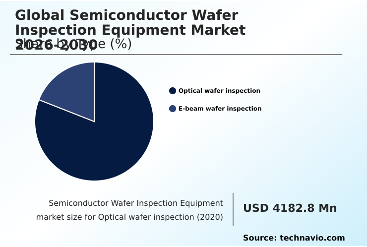
The Optical wafer inspection segment was valued at USD 5.72 billion in 2024 and showed a gradual increase during the forecast period.
Regional Analysis
APAC is estimated to contribute 74.9% to the growth of the global market during the forecast period.Technavio’s analysts have elaborately explained the regional trends and drivers that shape the market during the forecast period.

See How Semiconductor Wafer Inspection Equipment Market Demand is Rising in APAC Get Free Sample
The geographic landscape of the semiconductor wafer inspection equipment market is dominated by APAC, which captures approximately 74.9% of the incremental growth, fueled by its massive foundry and memory manufacturing capacity.
This region's insatiable demand for high-throughput inspection technologies is driven by the continuous pursuit of higher yields in complex processes like extreme ultraviolet lithography.
Concurrently, government-led initiatives in North America and Europe are reshaping the global supply chain, creating sustained demand for advanced optical and electron-beam inspection systems in new fabrication facilities.
North America is forecast to expand at a rate of 9.8%, outpacing Europe's 8.5% growth, reflecting significant capital expenditure in domestic manufacturing.
This regionalization trend diversifies the need for inspection tools, ranging from high-end platforms for sub-five nanometer nodes to robust systems for mature-node automotive and industrial applications.
Market Dynamics
Our researchers analyzed the data with 2025 as the base year, along with the key drivers, trends, and challenges. A holistic analysis of drivers will help companies refine their marketing strategies to gain a competitive advantage.
- A critical debate in the semiconductor industry centers on e-beam vs optical wafer inspection for ensuring quality. While optical methods offer high throughput, the challenge of defect detection for sub-three nanometer nodes often necessitates the superior resolution of e-beam technology. The complexity of inspecting three dimensional chip structures, particularly with the rise of heterogeneous integration, further complicates this choice.
- To address these challenges, the industry is increasingly leveraging AI in semiconductor defect classification, using advanced algorithms to differentiate critical anomalies from background noise with greater accuracy. This technological shift is pivotal for improving yield with wafer inspection, as it allows for faster root-cause analysis and proactive process adjustments.
- For instance, fabs that integrate AI-powered review systems have demonstrated an ability to reduce inspection cycle times by more than half compared to manual methods, directly impacting manufacturing efficiency. Ultimately, a hybrid approach combining the speed of optical scans with targeted e-beam analysis for critical defect review is becoming the standard for effective yield management in leading-edge fabrication.
What are the key market drivers leading to the rise in the adoption of Semiconductor Wafer Inspection Equipment Industry?
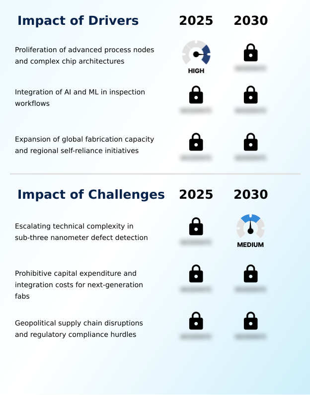
- The proliferation of advanced process nodes and complex chip architectures serves as a primary driver for the global semiconductor wafer inspection equipment market.
- The market is propelled by several key drivers, primarily the continuous push toward advanced process nodes. The transition to sub-five nanometer nodes increases the complexity of wafer patterns, making high-resolution inspection essential for functional yield.
- Secondly, the integration of machine learning models into inspection platforms has revolutionized defect classification, with some fabs reporting a 40% reduction in false positives, thereby minimizing costly production pauses. This hardware-software synergy enhances yield management strategies.
- A third driver is the global expansion of fabrication capacity, spurred by initiatives like the CHIPS Act.
- This has resulted in the construction of new facilities, each requiring a full suite of inspection tools, which has increased equipment procurement by 20% in supported regions.
What are the market trends shaping the Semiconductor Wafer Inspection Equipment Industry?
- The integration of physics-informed AI and deep learning architectures is a pervasive trend. It is reshaping traditional defect classification methodologies in the semiconductor industry.
- Key trends are reshaping the semiconductor wafer inspection equipment market, driven by technological and geopolitical shifts. The most significant trend is the integration of deep learning architectures for real-time defect classification, where automated systems are improving detection accuracy by up to 25% compared to legacy rule-based methods.
- Concurrently, the industry's move toward heterogeneous integration and 3D packaging necessitates a shift to full volumetric 3D metrology and advanced analytics platforms. This requires inspection tools capable of verifying through-silicon vias and micro-bumps with nanometer precision. A third major trend is the regionalization of fabrication capacity, which diversifies the demand for inspection equipment across both leading-edge and mature process nodes.
- This trend is also fostering the growth of localized service and support networks.
What challenges does the Semiconductor Wafer Inspection Equipment Industry face during its growth?
- The escalating technical complexity of defect detection at sub-three nanometer scales presents a significant and ongoing challenge to industry growth.
- The semiconductor wafer inspection equipment market faces several significant challenges. The primary technical hurdle is the difficulty of nanoscale defect detection at sub-three nanometer scales, where conventional optical methods reach their physical limits. This necessitates a shift to lower-throughput technologies like multi-beam e-beam inspection, which can increase wafer processing time by up to 50% in some cases.
- Another major restraint is the prohibitive capital expenditure, with a single advanced inspection tool costing tens of millions of dollars. This high cost consolidates manufacturing capabilities among a few large players. Finally, geopolitical supply chain disruptions and stringent export controls on advanced metrology tools create a fragmented and uncertain market, increasing operational costs and compliance burdens for equipment manufacturers.
Exclusive Technavio Analysis on Customer Landscape
The semiconductor wafer inspection equipment market forecasting report includes the adoption lifecycle of the market, covering from the innovator’s stage to the laggard’s stage. It focuses on adoption rates in different regions based on penetration. Furthermore, the semiconductor wafer inspection equipment market report also includes key purchase criteria and drivers of price sensitivity to help companies evaluate and develop their market growth analysis strategies.

Customer Landscape of Semiconductor Wafer Inspection Equipment Industry
Competitive Landscape
Companies are implementing various strategies, such as strategic alliances, semiconductor wafer inspection equipment market forecast, partnerships, mergers and acquisitions, geographical expansion, and product/service launches, to enhance their presence in the industry.
Applied Materials Inc. - Providers deliver advanced metrology and defect inspection solutions crucial for optimizing semiconductor fabrication yields and enabling next-generation process nodes.
The industry research and growth report includes detailed analyses of the competitive landscape of the market and information about key companies, including:
- Applied Materials Inc.
- ASML Holding NV
- Bruker Corp.
- Camtek Ltd.
- Carl Zeiss AG
- Cognex Corp.
- Hitachi Ltd.
- JEOL Ltd.
- KLA Corp.
- Lam Research Corp.
- Lasertec Corp
- Nanometrics Inc.
- Nikon Corp.
- Nova Ltd.
- NXP Semiconductors NV
- Onto Innovation Inc.
- Synopsys Inc.
- Teradyne Inc.
- Toray Industries Inc.
- TSI Inc.
Qualitative and quantitative analysis of companies has been conducted to help clients understand the wider business environment as well as the strengths and weaknesses of key industry players. Data is qualitatively analyzed to categorize companies as pure play, category-focused, industry-focused, and diversified; it is quantitatively analyzed to categorize companies as dominant, leading, strong, tentative, and weak.
Recent Development and News in Semiconductor wafer inspection equipment market
- In March, 2025, ASML Holding N.V. signed a strategic partnership with the research institute imec to advance semiconductor research, focusing on metrology and inspection advancements for next-generation node scaling.
- In February, 2025, Applied Materials, Inc. launched the SEMVision H20 defect review system, integrating AI-driven image recognition for faster, more accurate nanoscale defect detection in sub-three nanometer fabrication.
- In March, 2025, TSMC announced an expansion of its U.S. investment to approximately $165 billion, including new fabrication plants and advanced packaging facilities that will require comprehensive inspection suites.
- In December, 2024, Lasertec Corp. released the ABICS Series E320 EUV mask blank inspection system to support defect management and yield improvement for sub-five nanometer and beyond nodes.
Dive into Technavio’s robust research methodology, blending expert interviews, extensive data synthesis, and validated models for unparalleled Semiconductor Wafer Inspection Equipment Market insights. See full methodology.
| Market Scope | |
|---|---|
| Page number | 299 |
| Base year | 2025 |
| Historic period | 2020-2024 |
| Forecast period | 2026-2030 |
| Growth momentum & CAGR | Accelerate at a CAGR of 9.3% |
| Market growth 2026-2030 | USD 4350.6 million |
| Market structure | Fragmented |
| YoY growth 2025-2026(%) | 8.9% |
| Key countries | China, Taiwan, South Korea, Japan, India, Singapore, US, Canada, Mexico, Germany, UK, France, Italy, Spain, The Netherlands, Brazil, Argentina, Chile, Saudi Arabia, UAE, South Africa, Israel and Turkey |
| Competitive landscape | Leading Companies, Market Positioning of Companies, Competitive Strategies, and Industry Risks |
Research Analyst Overview
- The semiconductor wafer inspection equipment market is driven by the non-negotiable need for defect-free manufacturing at atomic scales. The transition to gate-all-around architectures and 3D NAND structures has made investment in advanced inspection a critical boardroom decision, directly impacting competitiveness. Technologies such as electron-beam inspection and high-numerical aperture EUV lithography are essential for nanoscale defect detection.
- The use of deep learning architectures and multi-beam e-beam inspection is no longer optional but a baseline requirement for high-volume manufacturing. Boardroom decisions now hinge on balancing the high capital expenditure of these platforms against the unacceptable cost of yield loss.
- For instance, deploying systems with physics-informed AI for automated defect classification has enabled some fabs to achieve a 30% reduction in processing time for failure analysis. This strategic adoption of technologies, including voltage contrast inspection and optical pattern inspection, is fundamental to achieving high-yield production in the era of sub-five nanometer nodes.
What are the Key Data Covered in this Semiconductor Wafer Inspection Equipment Market Research and Growth Report?
-
What is the expected growth of the Semiconductor Wafer Inspection Equipment Market between 2026 and 2030?
-
USD 4.35 billion, at a CAGR of 9.3%
-
-
What segmentation does the market report cover?
-
The report is segmented by Type (Optical wafer inspection, and E-beam wafer inspection), Application (Front-end process inspection, Back-end process inspection, Wafer defect inspection, and Yield management and failure analysis), End-user (Foundries, and IDMs) and Geography (APAC, North America, Europe, South America, Middle East and Africa)
-
-
Which regions are analyzed in the report?
-
APAC, North America, Europe, South America and Middle East and Africa
-
-
What are the key growth drivers and market challenges?
-
Proliferation of advanced process nodes and complex chip architectures, Escalating technical complexity in sub-three nanometer defect detection
-
-
Who are the major players in the Semiconductor Wafer Inspection Equipment Market?
-
Applied Materials Inc., ASML Holding NV, Bruker Corp., Camtek Ltd., Carl Zeiss AG, Cognex Corp., Hitachi Ltd., JEOL Ltd., KLA Corp., Lam Research Corp., Lasertec Corp, Nanometrics Inc., Nikon Corp., Nova Ltd., NXP Semiconductors NV, Onto Innovation Inc., Synopsys Inc., Teradyne Inc., Toray Industries Inc. and TSI Inc.
-
Market Research Insights
- The market dynamics are shaped by a strategic shift toward intelligent metrology and predictive analytics to enhance semiconductor fabrication quality. The integration of advanced analytics platforms enables fabs to improve yield management strategies, with some achieving a 15% faster ramp-to-yield on new process nodes.
- Concurrently, AI-driven systems are reducing false positives in defect classification by over 40%, optimizing operational efficiency and minimizing unnecessary production holds. This focus on software-hardware synergy is critical for managing the total cost of ownership, as manufacturers balance capital expenditure with the need for high-resolution nanoscale defect analysis.
- Furthermore, the emphasis on known-good-die strategies in advanced packaging workflows is reinforcing the need for robust, end-to-end quality assurance across the supply chain. These dynamics highlight a market where data-driven process control is becoming as crucial as the inspection hardware itself.
We can help! Our analysts can customize this semiconductor wafer inspection equipment market research report to meet your requirements.
 RIA -
RIA - 
