Atomic Force Microscopy Market Size 2026-2030
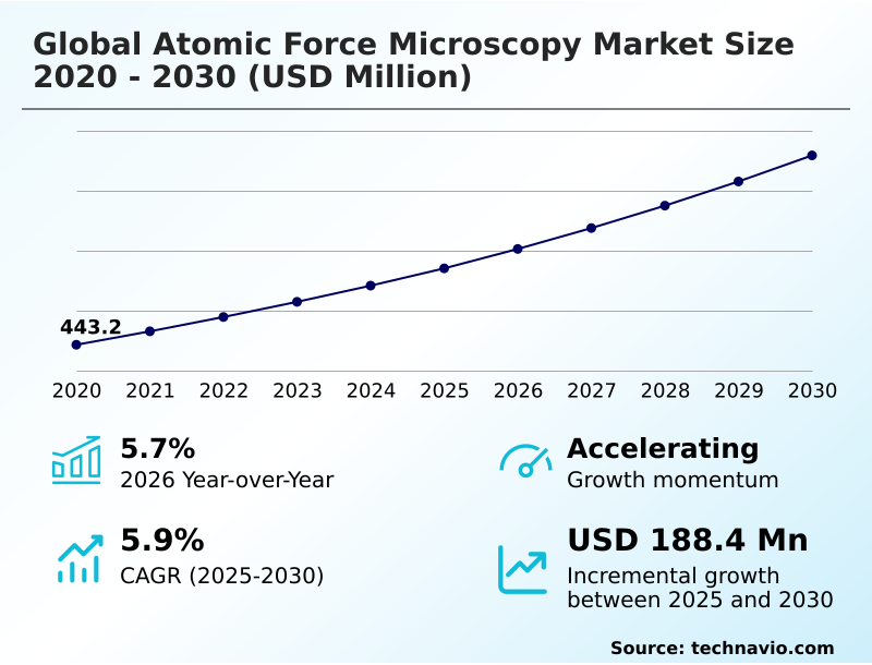
The atomic force microscopy market size is valued to increase by USD 188.4 million, at a CAGR of 5.9% from 2025 to 2030. Integration of artificial intelligence in metrology will drive the atomic force microscopy market.
Major Market Trends & Insights
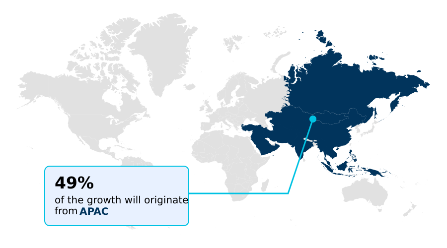
- APAC dominated the market and accounted for a 49% growth during the forecast period.
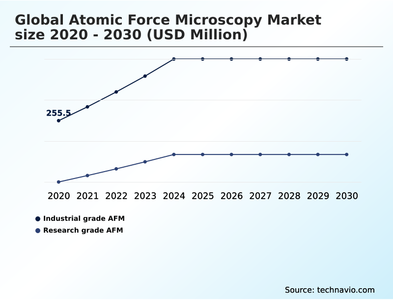
- By Type - Industrial grade AFM segment was valued at USD 323.7 million in 2024
- By Technology - Tapping mode segment accounted for the largest market revenue share in 2024
Market Size & Forecast
- Market Opportunities: USD 315.8 million
- Market Future Opportunities: USD 188.4 million
- CAGR from 2025 to 2030 : 5.9%
Market Summary
- The Atomic Force Microscopy Market is defined by its capacity for high-resolution imaging and nanoscale metrology, serving as a critical tool in materials science, semiconductor manufacturing, and biological research. Market momentum is sustained by the integration of artificial intelligence and robotics, which automates complex scan parameters and feedback loop adjustments, thereby improving data consistency.
- This push for automation addresses the persistent challenge of the operational skill gap. A key business scenario involves a semiconductor fabrication plant using automated AFM for inline defect classification on wafers, which enhances yield by identifying and correcting process deviations in near real-time.
- Furthermore, the convergence with other analytical techniques, known as correlative microscopy, provides a more holistic understanding of a sample's chemical and mechanical properties. While the technology offers unparalleled atomic resolution, its adoption is constrained by the high cost of instrumentation and the inherent trade-off between imaging speed and data quality.
- The market is evolving from a purely research-oriented tool to a vital component in advanced industrial quality control, enabling non-destructive testing of large samples and expanding its application in nanotechnology development.
What will be the Size of the Atomic Force Microscopy Market during the forecast period?
Get Key Insights on Market Forecast (PDF) Get Free Sample
How is the Atomic Force Microscopy Market Segmented?
The atomic force microscopy industry research report provides comprehensive data (region-wise segment analysis), with forecasts and estimates in "USD million" for the period 2026-2030, as well as historical data from 2020-2024 for the following segments.
- Type
- Industrial grade AFM
- Research grade AFM
- Technology
- Tapping mode
- Contact mode
- Non contact mode
- Others
- Application
- Semiconductors and electronics
- Life sciences and biology
- Material science and nanotechnology
- Others
- Geography
- APAC
- China
- Japan
- South Korea
- North America
- US
- Canada
- Mexico
- Europe
- Germany
- France
- UK
- Middle East and Africa
- Saudi Arabia
- UAE
- South Africa
- South America
- Brazil
- Argentina
- Colombia
- Rest of World (ROW)
- APAC
By Type Insights
The industrial grade afm segment is estimated to witness significant growth during the forecast period.
The industrial grade AFM segment is driven by the semiconductor industry's demand for high-throughput, automated metrology solutions. These systems, distinct from research grade AFM, are engineered for inline process control, emphasizing wafer cleanliness verification and reliability to support zero-defect manufacturing.
The evolution toward scan-by-recipe operations and automated defect classification has been pivotal, with advancements in vibration isolation and cantilever dynamics enabling a more than 15% reduction in measurement inconsistencies.
The focus on large-sample inspection and non-destructive testing of a 300 mm wafer without coupon-based sampling is reshaping quality control workflows.
This shift positions industrial systems as intelligent sensors essential for smart manufacturing, where topographical map data quality is decoupled from operator skill, facilitating robust surface characterization at scale.
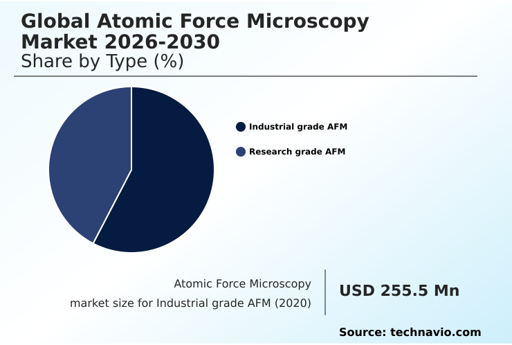
The Industrial grade AFM segment was valued at USD 323.7 million in 2024 and showed a gradual increase during the forecast period.
Regional Analysis
APAC is estimated to contribute 49% to the growth of the global market during the forecast period.Technavio’s analysts have elaborately explained the regional trends and drivers that shape the market during the forecast period.
See How Atomic Force Microscopy Market Demand is Rising in APAC Get Free Sample
The geographic landscape of the market is led by APAC, which accounts for over 40% of the market due to its dominance in semiconductor manufacturing.
The region's demand is heavily skewed toward industrial systems for large-sample inspection and inline process control.
In contrast, North America and Europe are significant hubs for advanced materials research and life sciences, driving innovation in nanomechanical data acquisition and bio-mechanical properties analysis.
For instance, the adoption of correlative microscopy in North American labs has accelerated drug discovery timelines. The strategic focus on large-sample analysis in European automotive R&D has resulted in a 10% reduction in material validation cycles for lightweight composites.
This regional specialization shapes development, with APAC focusing on throughput and automation, while Western markets prioritize experimental versatility and environmental control for applications involving geological samples and solid electrolyte interphase studies.
Market Dynamics
Our researchers analyzed the data with 2025 as the base year, along with the key drivers, trends, and challenges. A holistic analysis of drivers will help companies refine their marketing strategies to gain a competitive advantage.
- The evolution of the atomic force microscopy market is increasingly defined by specialized applications that address complex industrial and scientific challenges. For instance, atomic force microscopy for semiconductor inspection is no longer limited to offline analysis but is now a cornerstone of automated afm for quality control, especially for reviewing high aspect ratio features on wafers.
- Concurrently, correlative microscopy for life sciences is revolutionizing biomedical research by allowing scientists to measure bio-mechanical properties with afm while simultaneously observing cellular functions. The development of high-speed afm for large samples, particularly for large sample afm for wafer inspection, has addressed a critical throughput bottleneck, with some systems demonstrating a five-fold increase in scan speed over previous generations.
- A key enabler for this is the use of non-destructive testing with afm, which preserves high-value components. Technology selection is also crucial; tapping mode for soft biological samples is preferred for its gentle interaction, whereas contact mode for crystalline surfaces provides high-resolution data. The use of non-contact mode for defect review is standard in sensitive electronics applications.
- Innovations in afm for battery interface analysis and afm for polymer characterization are supporting the transition to sustainable energy and advanced materials.
- Furthermore, obtaining quantitative nanomechanical data from afm via an afm probe for nanomechanical mapping is vital for materials engineering, and the integration of afm with raman spectroscopy offers combined chemical and topographical insights, all driven by advances in ai integration in atomic force microscopy.
What are the key market drivers leading to the rise in the adoption of Atomic Force Microscopy Industry?
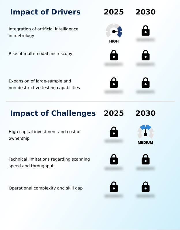
- The integration of artificial intelligence into metrology platforms is a primary driver for market growth, enhancing automation and data analysis capabilities.
- Market growth is primarily propelled by the integration of artificial intelligence and the rising demand for multi-modal characterization.
- AI-driven automation, which uses machine learning for real-time nanomanipulation and scan optimization, is a critical driver, effectively democratizing high-end nanometrology and enhancing reproducibility by more than 30%.
- This move toward intelligent, automated systems is transforming the technology into a robust sensor for smart manufacturing. A second major driver is the increasing requirement for correlative microscopy, which combines the tip-sample interaction of an AFM with other analytical methods.
- This approach is essential in pharmacology and material science, where understanding structure-function relationships is key.
- The migration from small, research-grade afm setups to large-sample, industrial-grade afm platforms for non-destructive testing also fuels the market, aligning with sustainability goals by eliminating material waste from destructive sampling.
What are the market trends shaping the Atomic Force Microscopy Industry?
- A key market trend is the accelerating adoption of robotic automation in metrology. This shift is driven by the industrial need for higher throughput and reproducibility in nanoscale analysis.
- Key market trends are centered on automation and functional integration to meet escalating industrial demands. The acceleration of robotic systems for high-throughput metrology is paramount, enabling autonomous probe exchange and scan parameter optimization, which has been shown to reduce operator-induced errors by up to 25%.
- This trend toward autonomous systems is crucial for achieving the stringent quality control required for angstrom-level nodes in semiconductor fabrication. Another significant trend is the convergence of correlative characterization techniques, such as combining a topographical map with hyperspectral analysis. This allows for a holistic view of advanced materials, a capability that improves material design cycle times by over 15%.
- The shift toward non-destructive, large-sample inspection of a full wafer surface further addresses the economic need to minimize waste and maximize yield in high-value manufacturing.
What challenges does the Atomic Force Microscopy Industry face during its growth?
- The substantial capital investment and high total cost of ownership for advanced instrumentation present a key challenge to broader market adoption.
- Despite its advanced capabilities, the market faces significant challenges, primarily the high capital investment and total cost of ownership. The sophisticated robotics and advanced piezoelectric actuators in state-of-the-art systems make them inaccessible for many smaller enterprises and academic labs.
- The recurring expense of specialized consumables, particularly high-quality probes and wear-resistant probes, adds to the operational burden, which can increase annual lab budgets by 10-15%. Another formidable challenge is the inherent trade-off between imaging speed and resolution; the slow scan time remains a bottleneck for high-volume applications, restricting its use for 100% inline inspection.
- Finally, the operational complexity and the associated skill gap create a barrier to adoption. While automation helps, the need for expert-level probe mechanics knowledge for troubleshooting and methods development remains, slowing broader market penetration.
Exclusive Technavio Analysis on Customer Landscape
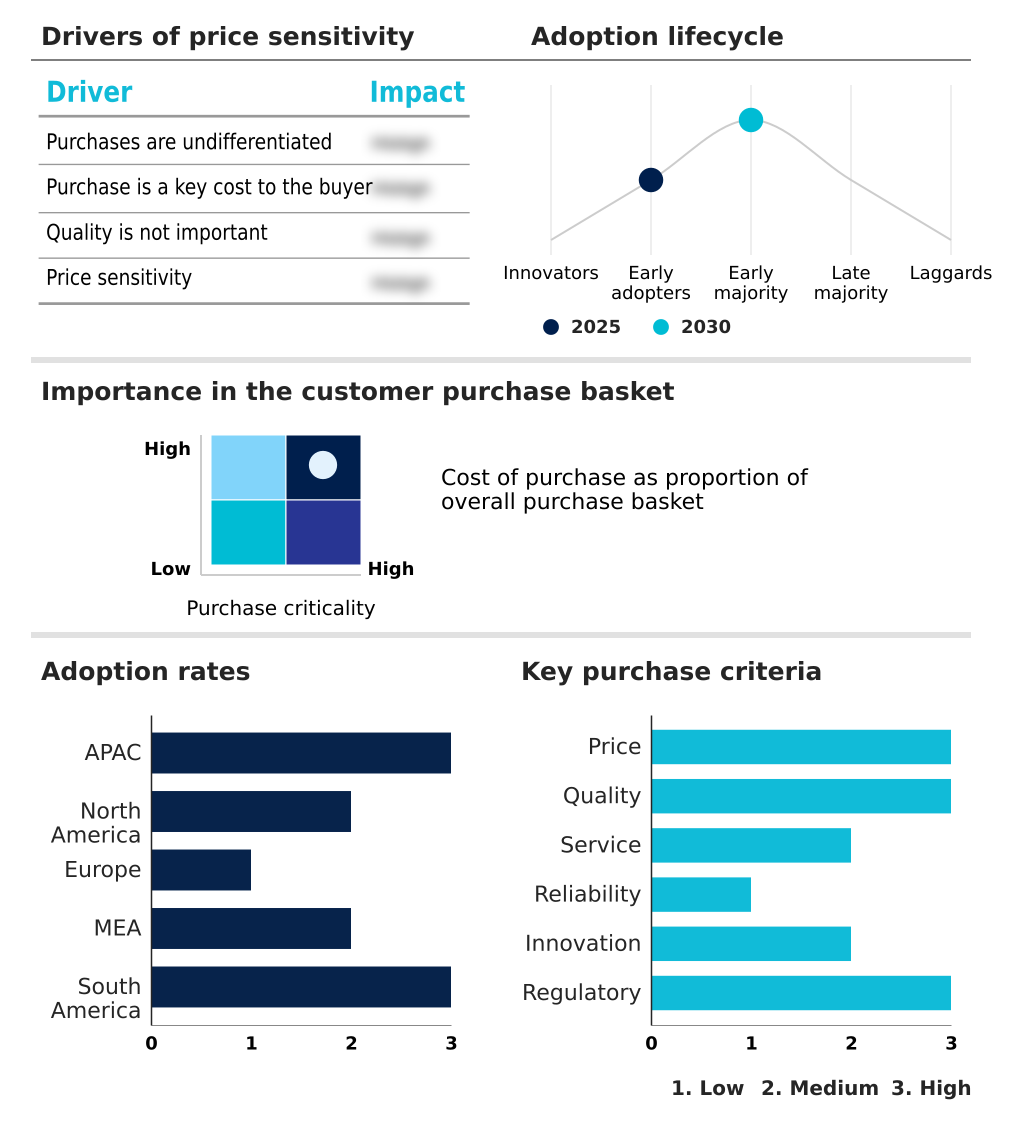
The atomic force microscopy market forecasting report includes the adoption lifecycle of the market, covering from the innovator’s stage to the laggard’s stage. It focuses on adoption rates in different regions based on penetration. Furthermore, the atomic force microscopy market report also includes key purchase criteria and drivers of price sensitivity to help companies evaluate and develop their market growth analysis strategies.
Customer Landscape of Atomic Force Microscopy Industry
Competitive Landscape
Companies are implementing various strategies, such as strategic alliances, atomic force microscopy market forecast, partnerships, mergers and acquisitions, geographical expansion, and product/service launches, to enhance their presence in the industry.
A.P.E. Research S.r.l. - Delivering advanced systems for high-resolution nanoscale imaging, the portfolio enables detailed mechanical property mapping and analysis for diverse biological and material science applications.
The industry research and growth report includes detailed analyses of the competitive landscape of the market and information about key companies, including:
- A.P.E. Research S.r.l.
- AFMWorkshop Inc.
- Angstrom Advanced Inc.
- Bruker Corp.
- Hitachi High Tech Corp.
- Molecular Vista
- Nanomagnetics Instruments
- Nanonics Imaging Ltd.
- Nanosurf AG
- NanoWorld AG
- NenoVision s.r.o.
- NT MDT Spectrum Group
- Oxford Instruments plc
- Park Systems Corp.
- WITec GmbH
Qualitative and quantitative analysis of companies has been conducted to help clients understand the wider business environment as well as the strengths and weaknesses of key industry players. Data is qualitatively analyzed to categorize companies as pure play, category-focused, industry-focused, and diversified; it is quantitatively analyzed to categorize companies as dominant, leading, strong, tentative, and weak.
Recent Development and News in Atomic force microscopy market
- In February, 2025, Park Systems Corp. launched the Park FX300 series at SEMICON Korea, introducing a fully automated system designed for 300 mm wafer analysis with optional integrated infrared spectroscopy for simultaneous chemical and topographical characterization.
- In April, 2025, Bruker Corp. co-hosted a technical workshop with the Arizona Imaging and Microanalysis Society to demonstrate the correlative microscopy capabilities of its Dimension Nexus platform, focusing on bio-mechanical mapping in life sciences.
- In June, 2025, Oxford Instruments plc released the Jupiter Discovery, a large-sample atomic force microscope engineered for high-speed scanning and atomic resolution, targeting both industrial and academic research applications requiring high throughput.
- In October, 2025, Nanosurf AG released new performance data for its WaveMode technology, highlighting its application in accelerating surface roughness measurements for high-throughput semiconductor metrology without causing tip damage.
Dive into Technavio’s robust research methodology, blending expert interviews, extensive data synthesis, and validated models for unparalleled Atomic Force Microscopy Market insights. See full methodology.
| Market Scope | |
|---|---|
| Page number | 294 |
| Base year | 2025 |
| Historic period | 2020-2024 |
| Forecast period | 2026-2030 |
| Growth momentum & CAGR | Accelerate at a CAGR of 5.9% |
| Market growth 2026-2030 | USD 188.4 million |
| Market structure | Fragmented |
| YoY growth 2025-2026(%) | 5.7% |
| Key countries | China, Japan, South Korea, Taiwan, India, Australia, US, Canada, Mexico, Germany, France, UK, Italy, The Netherlands, Spain, Saudi Arabia, UAE, South Africa, Israel, Turkey, Brazil, Argentina and Colombia |
| Competitive landscape | Leading Companies, Market Positioning of Companies, Competitive Strategies, and Industry Risks |
Research Analyst Overview
- The atomic force microscopy market is undergoing a significant transformation, moving from a specialized laboratory tool to an integrated component of industrial process control. This shift is driven by relentless innovation in nanoscale metrology, where the ability to achieve atomic resolution is now table stakes. The competitive frontier has moved to automation and multi-modal functionality, such as correlative microscopy.
- Boardroom decisions are increasingly influenced by the technology's impact on operational efficiency; for example, adopting automated metrology platforms with advanced feedback loop control and scan-by-recipe functions has been shown to improve data acquisition consistency by over 30% compared to manual operation.
- The demand for systems capable of non-destructive testing and large-sample analysis reflects a broader industrial trend toward sustainability and yield optimization.
- As such, the market's trajectory is defined by the practical application of high-resolution imaging and mechanical property mapping to solve real-world manufacturing and research challenges in areas like force spectroscopy and surface characterization, supported by robust environmental control and vibration isolation.
What are the Key Data Covered in this Atomic Force Microscopy Market Research and Growth Report?
-
What is the expected growth of the Atomic Force Microscopy Market between 2026 and 2030?
-
USD 188.4 million, at a CAGR of 5.9%
-
-
What segmentation does the market report cover?
-
The report is segmented by Type (Industrial grade AFM, and Research grade AFM), Technology (Tapping mode, Contact mode, Non contact mode, and Others), Application (Semiconductors and electronics, Life sciences and biology, Material science and nanotechnology, and Others) and Geography (APAC, North America, Europe, Middle East and Africa, South America)
-
-
Which regions are analyzed in the report?
-
APAC, North America, Europe, Middle East and Africa and South America
-
-
What are the key growth drivers and market challenges?
-
Integration of artificial intelligence in metrology, High capital investment and cost of ownership
-
-
Who are the major players in the Atomic Force Microscopy Market?
-
A.P.E. Research S.r.l., AFMWorkshop Inc., Angstrom Advanced Inc., Bruker Corp., Hitachi High Tech Corp., Molecular Vista, Nanomagnetics Instruments, Nanonics Imaging Ltd., Nanosurf AG, NanoWorld AG, NenoVision s.r.o., NT MDT Spectrum Group, Oxford Instruments plc, Park Systems Corp. and WITec GmbH
-
Market Research Insights
- The market's dynamics are shaped by a strong push toward automated metrology and multi-modal microscopy, driven by industrial demands for higher precision and efficiency. In semiconductor metrology, the adoption of autonomous probe exchange and advanced vibration isolation has led to a 20% improvement in measurement repeatability.
- Concurrently, the demand for hyperspectral mapping is growing, where correlating topographical data with chemical information reduces failure analysis timelines by over 30%. This convergence is essential for understanding complex polymer blends and two-dimensional crystals.
- As manufacturing moves toward angstrom-level nodes, the need for real-time nanomanipulation and high-throughput metrology intensifies, shifting the competitive landscape from pure resolution to integrated, intelligent characterization solutions that minimize the need for extensive sample preparation.
We can help! Our analysts can customize this atomic force microscopy market research report to meet your requirements.
 RIA -
RIA - 
