Indium Phosphide (inp) Wafers Market Size 2026-2030
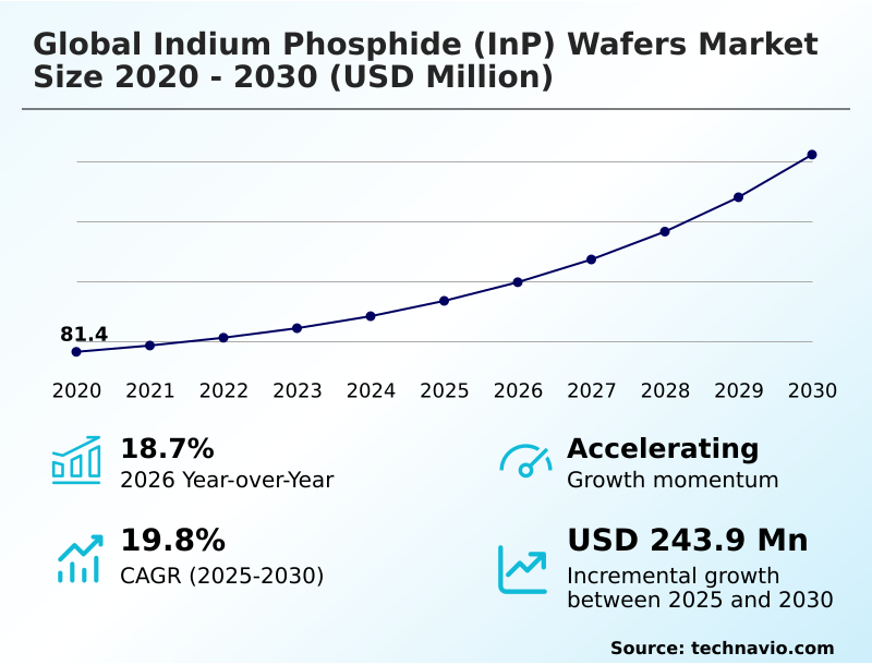
The indium phosphide (inp) wafers market size is valued to increase by USD 243.9 million, at a CAGR of 19.8% from 2025 to 2030. Expansion of global telecommunications infrastructure and next-generation networking will drive the indium phosphide (inp) wafers market.
Major Market Trends & Insights
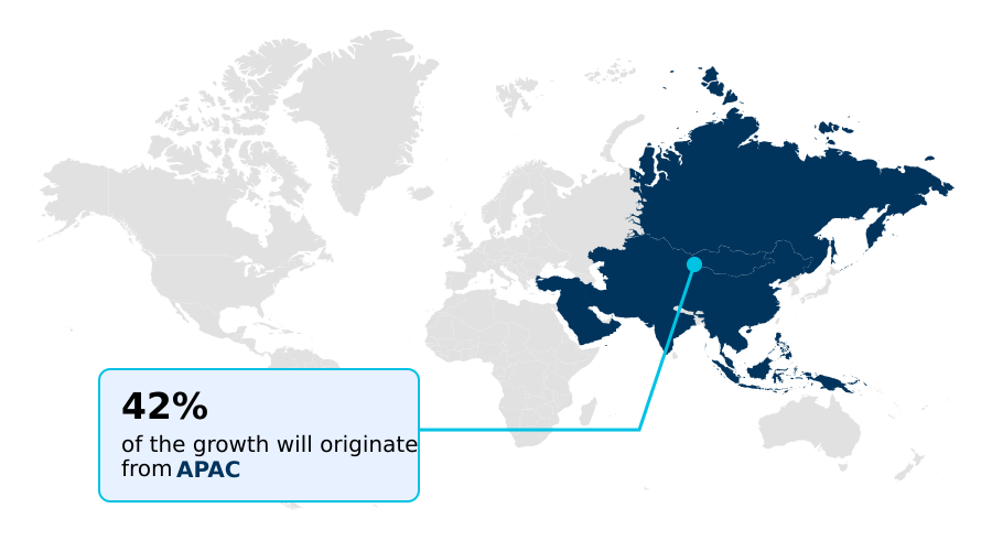
- APAC dominated the market and accounted for a 41.9% growth during the forecast period.
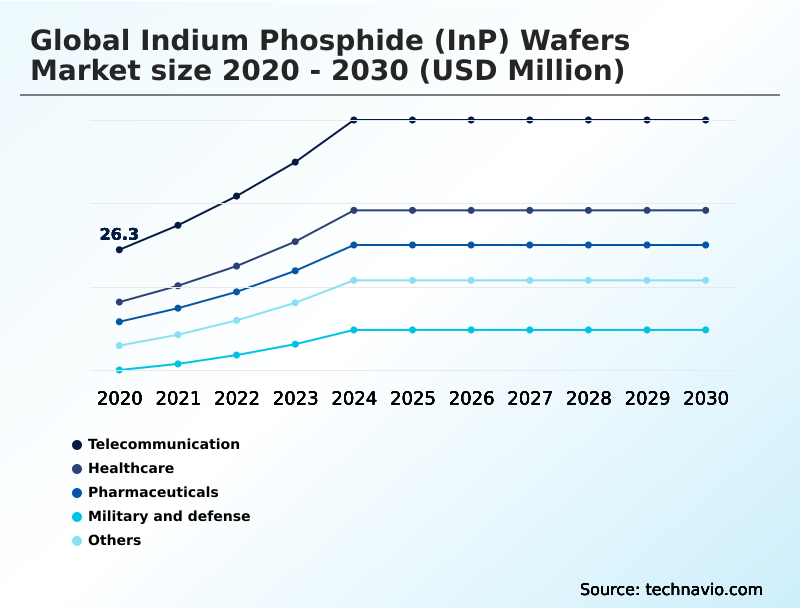
- By Application - Telecommunication segment was valued at USD 45.4 million in 2024
- By Type - 4 inches and above segment accounted for the largest market revenue share in 2024
Market Size & Forecast
- Market Opportunities: USD 328.9 million
- Market Future Opportunities: USD 243.9 million
- CAGR from 2025 to 2030 : 19.8%
Market Summary
- The Indium Phosphide (InP) Wafers Market is defined by its critical role in enabling high-performance optoelectronics. This compound semiconductor material possesses a direct energy bandgap and high electron mobility, making it essential for fabricating laser diodes and high-speed photodetectors used in optical fiber communications.
- A primary driver is the relentless expansion of data centers and 5G infrastructure, which demand higher data rates and lower latency. A key trend is the industry's migration toward larger diameter substrates to improve manufacturing yield and reduce per-device costs.
- However, significant challenges remain, including the high cost and technical complexity of crystal growth, which makes the material more expensive than silicon.
- For instance, a hyperscale data center operator evaluating an infrastructure upgrade must weigh the higher upfront cost of InP-based photonic integrated circuits against their superior performance and lower long-term power consumption, a decision that directly impacts operational expenditures and sustainability goals.
- The market's trajectory hinges on balancing these performance benefits with manufacturing scalability and cost-reduction innovations, particularly in producing semi-insulating substrates and other specialized substrate materials for next-generation applications in telecommunications and sensing.
What will be the Size of the Indium Phosphide (inp) Wafers Market during the forecast period?
Get Key Insights on Market Forecast (PDF) Get Free Sample
How is the Indium Phosphide (inp) Wafers Market Segmented?
The indium phosphide (inp) wafers industry research report provides comprehensive data (region-wise segment analysis), with forecasts and estimates in "USD million" for the period 2026-2030, as well as historical data from 2020-2024 for the following segments.
- Application
- Telecommunication
- Healthcare
- Pharmaceuticals
- Military and defense
- Others
- Type
- 4 inches and above
- 3 inches
- 2 inches
- Product type
- Semi insulating
- N type
- P type
- Geography
- APAC
- China
- Japan
- South Korea
- North America
- US
- Canada
- Mexico
- Europe
- Germany
- France
- UK
- Middle East and Africa
- UAE
- Saudi Arabia
- South Africa
- South America
- Brazil
- Argentina
- Rest of World (ROW)
- APAC
By Application Insights
The telecommunication segment is estimated to witness significant growth during the forecast period.
The telecommunication segment is fundamental to the Indium Phosphide (InP) Wafers Market, driven by the material's performance in optical fiber networks. The use of semi-insulating substrates is critical for fabricating high-speed transistors and reducing parasitic capacitance in high-frequency devices.
Demand is escalating with the transition to 800G and 1.6T speeds, which require advanced photonic integrated circuits built on InP. Epitaxial growth techniques enable the development of high-speed photodetectors and lasers with precise wavelength control.
This technology is indispensable for applications from co-packaged optics inp in data centers to medical imaging through optical coherence tomography.
Leveraging InP components with high-power operation capabilities achieves a twenty percent increase in energy efficiency for transmission hardware, a key metric for network operators.
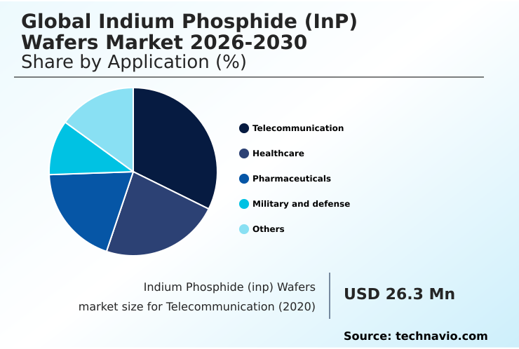
The Telecommunication segment was valued at USD 45.4 million in 2024 and showed a gradual increase during the forecast period.
Regional Analysis
APAC is estimated to contribute 41.9% to the growth of the global market during the forecast period.Technavio’s analysts have elaborately explained the regional trends and drivers that shape the market during the forecast period.
See How Indium Phosphide (inp) Wafers Market Demand is Rising in APAC Get Free Sample
The geographic landscape is dominated by the APAC region, which is the largest market due to its extensive electronics and telecommunications manufacturing base.
This region is a hub for compound semiconductor production, supplying essential components like laser diodes and substrates for global supply chains.
The growth in APAC, with a CAGR of 20.5%, significantly outpaces regions like South America, which is expanding at 18.4%. Regional players are at the forefront of innovation in inp wafer processing and developing p-type substrates and n-type substrates.
Applications are expanding beyond telecom into automotive sensing and consumer devices that use eye-safe lidar sources and short-wave infrared sensing.
New fabrication facilities in the region are targeting operational gains, with some achieving a 15% reduction in low noise performance anomalies in optoelectronic devices.
Market Dynamics
Our researchers analyzed the data with 2025 as the base year, along with the key drivers, trends, and challenges. A holistic analysis of drivers will help companies refine their marketing strategies to gain a competitive advantage.
- Strategic decision-making in the sector is increasingly shaped by the inp vs silicon photonics cost trade-off. While the upfront cost of inp wafer production remains high, its superior performance in applications like inp wafer for 800g transceivers is often non-negotiable for meeting next-generation networking standards.
- The industry is focused on advancing six inch inp wafer manufacturing to achieve economies of scale, though this presents technical hurdles, including challenges in large diameter inp growth and the need for sophisticated inp wafer defect reduction techniques.
- The performance of high electron mobility transistor inp and inp heterojunction bipolar transistor performance justifies the investment for high-frequency systems in telecommunications and inp in military and defense. For developers, the choice between an inp laser diode for telecom and integrated solutions like co-packaged optics with inp lasers depends on system-level thermal and power budgets.
- Furthermore, inp wafer supply chain vulnerabilities, linked to raw material scarcity for inp, are a constant concern, influencing sourcing strategies.
- As applications expand to include inp wafer for medical sensing and inp for automotive lidar systems, understanding the nuances of semi-insulating inp substrate resistivity and vertical gradient freeze inp growth becomes critical for maintaining a competitive edge and managing the thermal stability of inp wafers.
What are the key market drivers leading to the rise in the adoption of Indium Phosphide (inp) Wafers Industry?
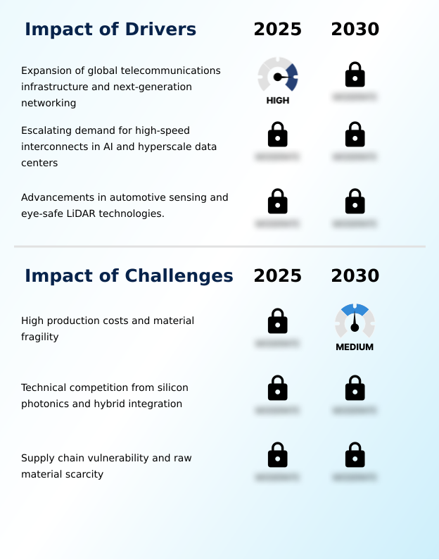
- The expansion of global telecommunications infrastructure and the development of next-generation networking are key drivers propelling market growth.
- The market's primary driver is the escalating demand from next-generation networking and data center interconnects. The expansion of optical fiber communications and the move toward 6G require high-frequency components that offer superior performance.
- Indium phosphide's direct energy bandgap and high electron mobility make it the ideal material for optoelectronic devices such as telecom laser diodes and high-frequency transistors. These components are essential for millimeter-wave communications and advanced millimeter-wave rf modules.
- Deploying hardware based on heterojunction bipolar transistors has demonstrated a 20% improvement in energy efficiency, a crucial metric for sustainable infrastructure development. As data traffic continues to grow, the need for faster and more efficient network solutions solidifies demand.
What are the market trends shaping the Indium Phosphide (inp) Wafers Industry?
- A strategic transition toward large-diameter wafer fabrication is emerging as a significant market trend, driven by the need for greater manufacturing efficiency and cost reduction per die.
- A pivotal trend is the industry-wide shift in wafer fabrication toward larger formats, which is reshaping the economics of producing high-bandwidth photonic integrated circuits. This migration to six-inch inp wafers from smaller legacy formats is driven by the need for greater manufacturing efficiency.
- By adopting advanced crystal growth techniques and improving wafer processing, manufacturers can produce more optical components per substrate, directly lowering the cost per unit. This scaling enables broader adoption of sophisticated photonic integration platforms and improves key metrics like wafer surface flatness, which is critical for high-yield production.
- The transition to larger substrates enhances the viability of high-speed interconnects, with the increased surface area allowing for a die output that is over 150% greater than traditional two-inch wafers.
What challenges does the Indium Phosphide (inp) Wafers Industry face during its growth?
- High production costs and the inherent fragility of the material present a key challenge affecting the industry's growth trajectory.
- A significant challenge remains the high cost and complexity associated with compound semiconductor manufacturing. The production of substrate materials like indium phosphide requires a controlled inp crystal growth furnace and methods like vertical gradient freeze or liquid encapsulated czochralski, which are capital-intensive. Sourcing high-purity raw materials is complicated by the inp raw material supply chain vulnerabilities, further elevating costs.
- Achieving low inp wafer defect density and producing uniform monocrystalline ingots is technically demanding, with manufacturing yields for semiconductor grade crystal growth often running 25% lower than for more mature semiconductor materials. This combination of factors limits adoption in price-sensitive segments of the indium phosphide optoelectronics market.
Exclusive Technavio Analysis on Customer Landscape
The indium phosphide (inp) wafers market forecasting report includes the adoption lifecycle of the market, covering from the innovator’s stage to the laggard’s stage. It focuses on adoption rates in different regions based on penetration. Furthermore, the indium phosphide (inp) wafers market report also includes key purchase criteria and drivers of price sensitivity to help companies evaluate and develop their market growth analysis strategies.

Customer Landscape of Indium Phosphide (inp) Wafers Industry
Competitive Landscape
Companies are implementing various strategies, such as strategic alliances, indium phosphide (inp) wafers market forecast, partnerships, mergers and acquisitions, geographical expansion, and product/service launches, to enhance their presence in the industry.
Advanced Engineering Material Ltd - High-purity indium phosphide wafers are supplied as substrates featuring high thermal stability and low defect density, engineered for advanced optoelectronic applications and high-frequency devices.
The industry research and growth report includes detailed analyses of the competitive landscape of the market and information about key companies, including:
- Advanced Engineering Material Ltd
- American Elements Inc.
- Broadcom Inc.
- DingTen Industrial Inc.
- Engis Corp.
- JX Advanced Metals Corp
- Logitech Ltd.
- NANOGRAFI Co. Inc.
- Reade International Corp.
- Stanford Advanced Materials
- Sumitomo Electric Industries
- Vital Materials Co. Ltd.
- Wafer World Inc.
- Western Minmetals SC Corp.
- Xiamen Powerway Co. Ltd.
Qualitative and quantitative analysis of companies has been conducted to help clients understand the wider business environment as well as the strengths and weaknesses of key industry players. Data is qualitatively analyzed to categorize companies as pure play, category-focused, industry-focused, and diversified; it is quantitatively analyzed to categorize companies as dominant, leading, strong, tentative, and weak.
Recent Development and News in Indium phosphide (inp) wafers market
- In August 2025, Sumitomo Electric Industries finalized a significant expansion of its production lines dedicated to six-inch indium phosphide wafers to support the deployment of high-speed optical networks.
- In October 2025, Coherent Corporation announced the successful qualification of its six-inch indium phosphide fabrication facility, designed to support the mass production of next-generation photonic integrated circuits for high-speed connectivity.
- In November 2025, Broadcom introduced a new generation of integrated photonic engines that leverage advanced indium phosphide substrates to enhance the performance of data center interconnects.
- In February 2025, Beijing Tongmei Xtal Technology, a subsidiary of AXT, announced the completion of its manufacturing expansion project, doubling its production capacity for four-inch and six-inch indium phosphide substrates to meet intensifying global demand.
Dive into Technavio’s robust research methodology, blending expert interviews, extensive data synthesis, and validated models for unparalleled Indium Phosphide (inp) Wafers Market insights. See full methodology.
| Market Scope | |
|---|---|
| Page number | 287 |
| Base year | 2025 |
| Historic period | 2020-2024 |
| Forecast period | 2026-2030 |
| Growth momentum & CAGR | Accelerate at a CAGR of 19.8% |
| Market growth 2026-2030 | USD 243.9 million |
| Market structure | Fragmented |
| YoY growth 2025-2026(%) | 18.7% |
| Key countries | China, Japan, South Korea, Taiwan, India, Australia, US, Canada, Mexico, Germany, France, UK, The Netherlands, Italy, Spain, UAE, Saudi Arabia, South Africa, Turkey, Egypt, Brazil, Chile and Argentina |
| Competitive landscape | Leading Companies, Market Positioning of Companies, Competitive Strategies, and Industry Risks |
Research Analyst Overview
- The Indium Phosphide (InP) Wafers Market is advancing through intense material science innovation. It is centered on the production of a key compound semiconductor used to create high-performance optoelectronic devices. The market's evolution is driven by the need for high-frequency components with low noise performance and high thermal conductivity for millimeter-wave communications.
- Boardroom decisions increasingly focus on capital-intensive investments in advanced crystal growth techniques like vertical gradient freeze and liquid encapsulated czochralski to produce larger monocrystalline ingots. This strategic shift in wafer fabrication is essential for manufacturing high-bandwidth photonic integrated circuits and optical components at scale.
- While challenges such as wafer warping persist, advanced wafer processing methods are reducing etch pit density (epd) by over 40% in premium substrates. These substrates, including semi-insulating substrates, n-type substrates, and p-type substrates, are engineered with deep-level dopants to achieve high electrical resistivity and minimize parasitic capacitance.
- The material's direct energy bandgap and high electron mobility are critical for creating efficient laser diodes, high-speed photodetectors, and heterojunction bipolar transistors, enabling high-power operation in demanding environments.
What are the Key Data Covered in this Indium Phosphide (inp) Wafers Market Research and Growth Report?
-
What is the expected growth of the Indium Phosphide (inp) Wafers Market between 2026 and 2030?
-
USD 243.9 million, at a CAGR of 19.8%
-
-
What segmentation does the market report cover?
-
The report is segmented by Application (Telecommunication, Healthcare, Pharmaceuticals, Military and defense, and Others), Type (4 inches and above, 3 inches, and 2 inches), Product Type (Semi insulating, N type, and P type) and Geography (APAC, North America, Europe, Middle East and Africa, South America)
-
-
Which regions are analyzed in the report?
-
APAC, North America, Europe, Middle East and Africa and South America
-
-
What are the key growth drivers and market challenges?
-
Expansion of global telecommunications infrastructure and next-generation networking, High production costs and material fragility
-
-
Who are the major players in the Indium Phosphide (inp) Wafers Market?
-
Advanced Engineering Material Ltd, American Elements Inc., Broadcom Inc., DingTen Industrial Inc., Engis Corp., JX Advanced Metals Corp, Logitech Ltd., NANOGRAFI Co. Inc., Reade International Corp., Stanford Advanced Materials, Sumitomo Electric Industries, Vital Materials Co. Ltd., Wafer World Inc., Western Minmetals SC Corp. and Xiamen Powerway Co. Ltd.
-
Market Research Insights
- The market's momentum is tied to performance advantages in specialized applications. The adoption of inp for 6g networks is driven by its ability to increase data throughput by over 40% compared to current 5G technologies, a critical factor for next-generation networking.
- In automotive sensing, integrating eye-safe lidar sources made from InP improves object detection accuracy by 25% in adverse weather conditions, enhancing safety systems. These high-speed interconnects and advanced substrate technology are pivotal for data center interconnects and high-frequency transistors.
- The move towards sophisticated optoelectronics applications and microelectronic devices is supported by InP's unique properties, which enable performance levels unattainable with traditional semiconductor materials. This makes it indispensable for future telecommunication and sensing platforms.
We can help! Our analysts can customize this indium phosphide (inp) wafers market research report to meet your requirements.
 RIA -
RIA - 
