Lithography Systems Market Size 2024-2028
The lithography systems market size is forecast to increase by USD 34.26 billion at a CAGR of 18% between 2023 and 2028.
- The market is experiencing significant growth due to several key drivers. One of the primary factors is the increasing investment in new fabrication facilities worldwide, which necessitates the adoption of advanced lithography systems to keep up with the demand for smaller, more intricate semiconductor designs. Another trend in the market is the increasing sizes of wafers, which require lithography systems with higher resolution and precision. However, constructing EUV lithography systems poses technical challenges, including the high cost of EUV sources and Construction and the complexity of EUV optics. Ultrahigh-precision photolithography tools, such as ArF immersion and ArF dry systems, are essential for manufacturing semiconductor devices with sub-micron features. These challenges are being addressed through ongoing research and development efforts, which are expected to drive market growth in the coming years. Overall, the Market is poised for strong expansion, driven by these key trends and the ever-evolving demands of the semiconductor industry.
What will be the Size of the Market During the Forecast Period?

- The market is a significant segment of the semiconductor industry, playing a crucial role in the production of Semiconductor Devices, including those used in Consumer Electronics and Smart Devices with 5G Connections. The market is driven by the adoption of advanced technologies like Next-Gen Advanced Technology, MEMS, Deep UV Lithography, LED and Extreme Ultraviolet (EUV) lithography. Lithography Technology is essential in Semiconductor FABs for creating patterns on Integrated Circuits and High-Definition Panels.
- Yield and Defect are critical factors affecting the market's growth. Alois Senefelder, the inventor of lithography in 1796, initiated the printing process using a chemical substance sensitive to light. Since then, lithography has evolved, with technologies like Wireless Control, Miniaturization Trend, and Lithography Technology's latest developments, such as EUV lithography, shaping the industry. Chipmakers continue to prioritize image quality and wavelengths to meet the demands of the Semiconductor industry and communication devices. Optical Projection Lithography and Deep UV Lithography are also key technologies in the market.
How is this market segmented and which is the largest segment?
The market research report provides comprehensive data (region-wise segment analysis), with forecasts and estimates in "USD billion" for the period 2024-2028, as well as historical data from 2018-2022 for the following segments.
- Technology
- ArF immersion lithography systems
- EUV lithography systems
- KrF lithography systems
- ArF dry lithography systems
- i-line lithography systems
- End-user
- IDMs
- Pureplay foundries
- Geography
- APAC
- China
- Japan
- South Korea
- North America
- US
- Europe
- South America
- Middle East and Africa
- APAC
By Technology Insights
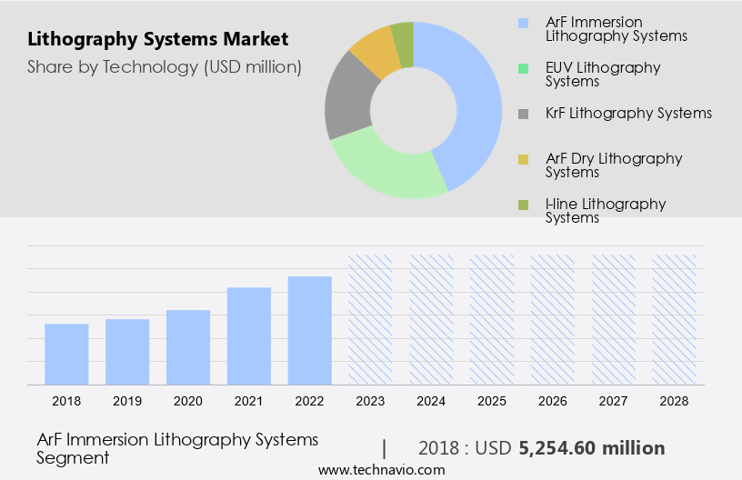
- The ArF immersion lithography systems segment is estimated to witness significant growth during the forecast period.
Semiconductor Lithography Equipment plays a pivotal role in the production of semiconductor devices, including consumer electronics and smart devices with 5G connections. The semiconductor fabrication process relies on advanced lithography technology to achieve high yield and minimize defects in the manufacturing of integrated circuits and high-definition panels. Next-gen advanced technologies like deep UV lithography and extreme ultraviolet lithography are driving innovation in the industry. Chipmakers and fabless firms leverage lithography solutions for miniaturization trend in semiconductor sales, particularly in the development of micro-electro mechanical systems, nanotechnology, and optoelectronics. The printing process, initiated by Alois Senefelder's invention of lithography in 1796, has evolved significantly, with optical projection lithography and EUV lithography becoming the industry standards.
Geopolitical scenarios, such as the Biden Administration's CHIPS Bill, influence the market dynamics. Machine learning and artificial intelligence are also being integrated into lithography systems to improve image quality and wavelength control. Additionally, emerging technologies like 3D printing and wireless control are shaping the future of semiconductor manufacturing.
Get a glance at the market report of share of various segments Request Free Sample
The ArF immersion lithography systems segment was valued at USD 5.25 billion in 2018 and showed a gradual increase during the forecast period.
Regional Analysis
- APAC is estimated to contribute 74% to the growth of the global market during the forecast period.
Technavio's analysts have elaborately explained the regional trends and drivers that shape the market during the forecast period.

For more insights on the market share of various regions Request Free Sample
Lithography systems play a pivotal role in the semiconductor industry, enabling the production of intricate microfabrications for various applications, including foundry, memory, electrification for Electric Vehicle technology, and advanced driver-assistance systems (ADAS). Ultrahigh-precision photolithography tools, such as ArF immersion and ArF dry systems, are essential for manufacturing semiconductor devices with sub-micron features. These advanced lithography systems employ sensors and pattern recognition technologies to ensure accuracy and consistency. Moreover, the integration of AI and ML in lithography tools enhances their capabilities, allowing for real-time process optimization and defect detection. The semiconductor manufacturing sector is witnessing significant capital investment in extreme ultraviolet (EUV) lithography and advanced packaging technologies to meet the increasing demand for smaller, more efficient semiconductor devices. These advancements will continue to drive the growth of the market.
Market Dynamics
Our researchers analyzed the data with 2023 as the base year, along with the key drivers, trends, and challenges. A holistic analysis of drivers will help companies refine their marketing strategies to gain a competitive advantage.
What are the key market drivers leading to the rise in adoption of Lithography Systems Market?
Growing investment in new fabs is the key driver of the market.
- The market is experiencing significant growth due to the expanding semiconductor industry and the increasing adoption of advanced technologies in consumer electronics. Semiconductor Devices, including Integrated Circuits (ICs) and Micro-Electro Mechanical Systems (MEMS), are integral to the production of smart devices, communication devices, and next-gen advanced technologies such as 5G connections and High-Definition Panels. To meet the rising demand for these components, semiconductor fabs are investing in new facilities and expanding existing ones. These fabs manufacture ICs either through in-house design by IDMs or through outsourcing to pureplay foundries.
- The miniaturization trend in technology and the development of next-generation lithography technologies, such as Extreme Ultraviolet (EUV) Lithography and Deep UV Lithography, are crucial to maintaining high yield and reducing defects. Geopolitical scenarios, such as the Biden Administration's CHIPS Bill, are also impacting the market dynamics. The printing process, which involves the transfer of patterns onto silicon wafers using light, has evolved significantly since its inception by Alois Senefelder in the late 18th century. Today, lithography technology employs wavelengths ranging from deep UV to EUV, and incorporates advanced technologies like wireless control, machine learning, and artificial intelligence to improve image quality.
What are the market trends shaping the Lithography Systems Market?
Increasing sizes of wafers is the upcoming trend in the market.
- The market is experiencing significant growth due to the increasing demand for advanced semiconductor devices, particularly in the consumer electronics sector, driven by the adoption of smart devices and the rollout of 5G connections. The semiconductor industry is focusing on next-gen advanced technology, such as Extreme Ultraviolet (EUV) lithography and Deep UV lithography, to meet the miniaturization trend and maintain high yield and defect levels. Chipmakers and fabless firms are investing heavily in these technologies to produce high-definition panels, integrated circuits, and Micro-Electro Mechanical Systems (MEMS) using nanotechnology and optoelectronics. The printing process, a crucial aspect of semiconductor manufacturing, has evolved from Alois Senefelder's invention of lithography in 1796 to the current optical lithography solutions and EUV lithography.
- The Biden Administration's CHIPS Bill and geopolitical scenarios have added impetus to the industry's growth. One of the major trends is the increasing use of 450-mm wafers, which have a larger surface area, enabling the production of a higher number of chips at lower manufacturing costs. The G450C consortium, comprising these industry leaders, is a significant undertaking to develop 450-mm wavelengths and wireless control systems for high-definition panels and integrated circuits. Semiconductor sales are expected to grow further with the integration of machine learning, artificial intelligence, the Internet of Things, 3D printing, and other advanced technologies.
What challenges does Lithography Systems Market face during its growth?
Technical challenges regarding the construction of EUV lithography systems is a key challenge affecting the market growth.
- EUV lithography systems, which utilize extreme ultraviolet light at a wavelength of 13.5nm for semiconductor fabrication, have long been anticipated as the next-gen advanced technology for high-volume manufacturing of semiconductor devices. The transition from conventional photolithography systems using exposure wavelengths of 248nm and 193nm to EUV lithography is imminent. However, the complexity of manufacturing EUV lithography systems poses significant challenges, delaying their commercialization on a global scale. EUV lithography represents a major leap forward in semiconductor manufacturing technology. The process involves generating EUV light through the excitation of a gas discharge, which is then used to expose photoresist on a semiconductor wafer.
- This results in higher resolution and improved image quality, enabling the miniaturization trend in semiconductor devices, including smartphones, consumer electronics, and communication devices with 5G connections. The semiconductor industry is undergoing a transformation, driven by the increasing adoption of semiconductor devices in various applications, from automotive and industrial to consumer electronics and telecommunications. Chipmakers and fabless firms are investing heavily in EUV lithography technology to meet the growing demand for high-performance, energy-efficient, and cost-effective semiconductor solutions. EUV lithography systems are essential for the production of high-definition panels, integrated circuits, micro-electro mechanical systems (MEMS), and nanotechnology applications. The challenges associated with EUV lithography, such as high cost, complex manufacturing processes, and defect management, are being addressed through next-gen advanced technology, including wireless control, machine learning, and artificial intelligence.
Exclusive Customer Landscape
The market forecasting report includes the adoption lifecycle of the market, covering from the innovator's stage to the laggard's stage. It focuses on adoption rates in different regions based on penetration. Furthermore, the market report also includes key purchase criteria and drivers of price sensitivity to help companies evaluate and develop their market growth analysis strategies.

Customer Landscape
Key Companies & Market Insights
Companies are implementing various strategies, such as strategic alliances, market forecast, partnerships, mergers and acquisitions, geographical expansion, and product/service launches, to enhance their presence in the market. The market research and growth report includes detailed analyses of the competitive landscape of the market and information about key companies, including:
- Advantest Corp.
- ASML
- Canon Inc.
- EV Group
- JEOL Ltd
- Neutronix Quintel
- Nikon Corp.
- NuFlare Technology Inc.
- Onto Innovation Inc.
- Raith GmbH
- Shanghai Micro Electronics Equipment Group Co. Ltd.
- SK Inc.
- SUSS MICROTEC SE
- Veeco Instruments Inc.
Qualitative and quantitative analysis of companies has been conducted to help clients understand the wider business environment as well as the strengths and weaknesses of key market players. Data is qualitatively analyzed to categorize companies as pure play, category-focused, industry-focused, and diversified; it is quantitatively analyzed to categorize companies as dominant, leading, strong, tentative, and weak.
Research Analyst Overview
The market is witnessing significant growth due to the increasing demand for Semiconductor Devices, particularly in Consumer Electronics and Smart Devices. The adoption of these devices, fueled by the rise of 5G Connections, is driving the need for advanced Semiconductor FABs and Lithography Technology. Next-Gen Advanced Technology, such as Deep UV Lithography and Optical Projection Lithography, is at the forefront of this growth. Chipmakers and fabless firms are investing heavily in these technologies to produce high-definition panels, mixed signal integrated circuits, Wafers, and Micro-Electro Mechanical Systems (MEMS) using nanotechnology and optoelectronics. Miniaturization trends and the development of High-Definition Panels, Integrated Circuits, and Micro-Electro Mechanical Systems are also contributing to the market's expansion. Key players in the market include chipmakers and fabless firms.
EUV Lithography, a next-generation technology, is gaining popularity due to its ability to print smaller features and higher resolution. The semiconductor industry is also exploring Extreme Ultraviolet Lithography and Nanotechnology for even more advanced manufacturing processes. Geopolitical Scenarios, such as the Biden Administration's CHIPS Bill, Silicone carbide, are also impacting the market. The bill aims to boost semiconductor sales and manufacturing in the US, potentially leading to increased demand for Lithography Systems. The printing process, a crucial aspect of Lithography Systems, is undergoing significant advancements, with Wireless Control and Machine Learning being integrated to improve yield and reduce defects.
|
Market Scope |
|
|
Report Coverage |
Details |
|
Page number |
172 |
|
Base year |
2023 |
|
Historic period |
2018-2022 |
|
Forecast period |
2024-2028 |
|
Growth momentum & CAGR |
Accelerate at a CAGR of 18% |
|
Market growth 2024-2028 |
USD 34.26 billion |
|
Market structure |
Concentrated |
|
YoY growth 2023-2024(%) |
15.7 |
|
Key countries |
Taiwan, South Korea, China, US, and Japan |
|
Competitive landscape |
Leading Companies, Market Positioning of Companies, Competitive Strategies, and Industry Risks |
What are the Key Data Covered in this Market Research and Growth Report?
- CAGR of the market during the forecast period
- Detailed information on factors that will drive the market growth and forecasting between 2024 and 2028
- Precise estimation of the size of the market and its contribution of the market in focus to the parent market
- Accurate predictions about upcoming market growth and trends and changes in consumer behaviour
- Growth of the market across APAC, North America, Europe, South America, and Middle East and Africa
- Thorough analysis of the market's competitive landscape and detailed information about companies
- Comprehensive analysis of factors that will challenge the growth of market companies
We can help! Our analysts can customize this market research report to meet your requirements. Get in touch
 RIA -
RIA - 
