Semiconductor Glass Wafer Market Size 2025-2029
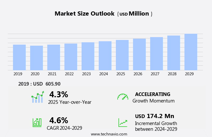
The semiconductor glass wafer market size is forecast to increase by USD 174.2 million, at a CAGR of 4.6% between 2024 and 2029.
- The market is experiencing significant growth, driven by the emergence of advanced and compact consumer electronic devices. The increasing proliferation of Internet of Things (IoT) and connected devices is fueling this demand, as these technologies rely heavily on semiconductor components. The use of synthetic quartz in construction is rapidly growing, as it offers a durable and aesthetically appealing alternative for countertops, flooring, and other surfaces, combining strength with design versatility. However, high inventory levels in the supply chain pose a challenge to market participants. These excess stocks can lead to price erosion and reduced profitability, necessitating effective inventory management strategies.
- Companies must navigate these dynamics to capitalize on market opportunities and maintain competitiveness. Strategic partnerships, innovation, and operational efficiency will be key differentiators in this competitive landscape. As IoT integrates data communication, hardware design, storage, and mining, semiconductor wafer polishing and grinding equipment play a crucial role in ensuring the precise manufacturing of semiconductor glass wafers.
What will be the Size of the Semiconductor Glass Wafer Market during the forecast period?
- The market is driven by the continuous advancement of microelectronics technology, with key trends including the adoption of low-k dielectrics and wafer process optimization. Chemical mechanical polishing and atomic layer deposition are essential techniques for enhancing wafer yield and ensuring high-quality single crystal silicon. Nano-structured glasses, such as ultra-thin oxide and alkali-aluminosilicate, play a crucial role in the production of advanced semiconductor devices. Manufacturers employ various etching techniques, including dry etching, plasma etching, and wet etching, for precise wafer fabrication. Thermal oxidation and chemical vapor deposition are essential processes for creating high-k dielectrics and doped glasses. Wafer defect analysis and metrology are critical for maintaining wafer quality control.
- Flexible glass, such as quartz and borosilicate, is gaining popularity in the semiconductor industry due to its potential for use in flexible electronics. Epitaxial growth and ion implantation are other essential processes for creating advanced semiconductor materials. Overall, the market is characterized by ongoing innovation and the pursuit of higher performance, lower power consumption, and smaller form factors.
How is this Semiconductor Glass Wafer Industry segmented?
The semiconductor glass wafer industry research report provides comprehensive data (region-wise segment analysis), with forecasts and estimates in "USD million" for the period 2025-2029, as well as historical data from 2019-2023 for the following segments.
- Type
- Borosilicate glass
- Quartz
- Fused silica
- Application
- Consumer electronics
- Automotive
- Industrial
- Aerospace and defense
- Others
- Technology
- Polished glass wafers
- Coated glass wafers
- Bonded glass wafers
- Etched glass wafers
- Product Type
- Less than 100 mm
- 100 mm to 200 mm
- 200 mm to 300 mm
- Above 300 mm
- Geography
- North America
- US
- Canada
- Europe
- France
- Germany
- UK
- APAC
- China
- India
- South Korea
- Taiwan
- South America
- Brazil
- Rest of World (ROW)
- North America
By Type Insights
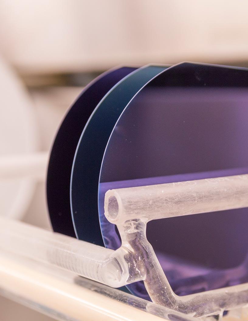
The borosilicate glass segment is estimated to witness significant growth during the forecast period. Borosilicate glass plays a pivotal role in the semiconductor industry, particularly in the production of glass wafer substrates. This material's properties significantly influence the market's growth and evolution. Among various borosilicate glass types, low-alkali borosilicate glass is a prominent choice for semiconductor applications. Its low alkali content, resulting from the absence or minimal presence of sodium and potassium ions, is crucial for semiconductor manufacturing. This reduced ion migration minimizes contamination and enhances the overall process's reliability and efficiency. The semiconductor wafer supply chain relies on the thermal stability of the glass wafers. Wafer thermal stability is essential for maintaining consistent wafer processing and ensuring the uniformity of the semiconductor devices.
Wafer doping, a critical process in semiconductor manufacturing, requires precise control over the wafer's resistivity. Borosilicate glass's chemical properties, such as its high resistivity and excellent thermal stability, make it an ideal choice for semiconductor wafer fabrication. Wafer cleaning is another essential process in semiconductor manufacturing. Borosilicate glass's high mechanical strength and resistance to thermal shock make it suitable for withstanding the rigorous cleaning processes. Wafer research and modeling play a vital role in optimizing wafer design and improving wafer performance. Wafer simulation and characterization techniques help identify potential issues and enhance the overall quality of the semiconductor devices.
Wafer thickness, flatness, and uniformity are essential factors in semiconductor manufacturing. Thin film deposition and wafer development techniques enable the creation of precise wafer specifications. Wafer bonding, a critical process in semiconductor packaging, requires high-quality glass substrates with excellent surface flatness and mechanical strength. The market's demand is driven by the increasing demand for advanced semiconductor devices. Wafer reliability, lifetime, and yield are crucial factors in meeting the market's demands. Wafer testing and inspection techniques ensure the quality of the final products. Glass substrates, an essential component of semiconductor devices, require careful handling and storage to maintain their integrity. Transparent quartz tubes provide advantages over ordinary glass, including maximum light transmission and resistance to high temperatures.
In summary, borosilicate glass's unique properties, such as its low alkali content, thermal stability, and mechanical strength, make it a vital component in the semiconductor industry. Its influence extends to various aspects of semiconductor manufacturing, from wafer fabrication to packaging and handling. The market's dynamics and trends are shaped by the evolving demands for advanced semiconductor devices and the continuous efforts to improve wafer quality and performance.
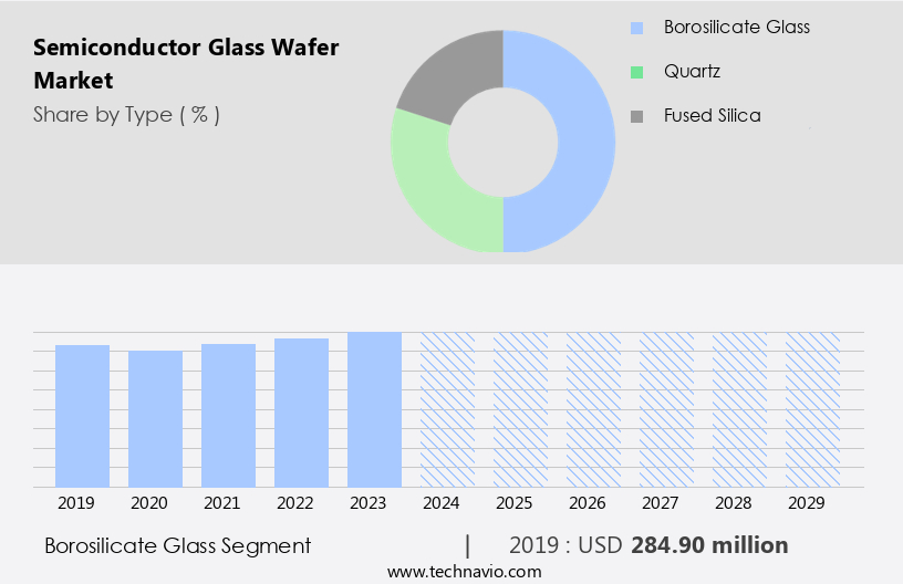
The Borosilicate glass segment was valued at USD 284.90 million in 2019 and showed a gradual increase during the forecast period.
Regional Analysis
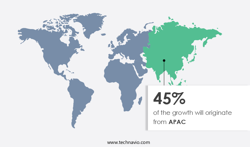
APAC is estimated to contribute 45% to the growth of the global market during the forecast period.Technavio's analysts have elaborately explained the regional trends and drivers that shape the market during the forecast period.
The market is driven by the increasing demand for advanced electronics and the continuous evolution of technology. Wafer standards, such as silicon wafers, play a crucial role in the manufacturing process. Thermal stability is essential for wafer supply chain efficiency, ensuring consistent product quality. Wafer doping, resistivity, cleaning, research, modeling, conductivity, orientation, mechanical strength, testing, fabrication, reliability, flatness, analysis, cost, simulation, stress, demand, optical properties, bonding, specifications, chemical properties, microstructure, crystallographic orientation, thickness, characterization, processing, diameter, thin film deposition, development, yield, defect, technology, packaging, handling, surface roughness, innovation, lifetime, uniformity, and storage are all integral aspects of the industry. Transparent quartz tubes are increasingly being used in photovoltaic applications due to their excellent thermal and electrical insulation properties, which help improve the efficiency of solar panels. With the ongoing focus on renewable energy sources and the continuous advancements in photovoltaic technology, the demand for transparent quartz tubes in this segment is expected to increase significantly.
APAC, with its abundance of raw materials and low production costs, dominates the global market. Major consumer electronics and automotive manufacturers in countries like China, South Korea, and Japan contribute significantly to the region's market share. The semiconductor manufacturing industry's growth is fueled by the continuous development of glass substrates and wafer quality, leading to increased wafer demand and innovation.
Market Dynamics
Our researchers analyzed the data with 2024 as the base year, along with the key drivers, trends, and challenges. A holistic analysis of drivers will help companies refine their marketing strategies to gain a competitive advantage.
What are the Semiconductor Glass Wafer market drivers leading to the rise in the adoption of Industry?
- The emergence of advanced and compact consumer electronic devices serves as the primary catalyst for market growth, as technology continues to evolve and shrink in size, providing consumers with increasingly convenient and feature-rich products. The market is experiencing significant growth due to the increasing demand for advanced electronic devices. Wafer fabrication and testing processes are crucial in ensuring wafer reliability and flatness for producing high-quality semiconductor wafers. Wafer analysis, simulation, and bonding are essential steps in the manufacturing process to maintain precise wafer specifications. Wafer optical properties, such as refractive index and transparency, are vital for the production of semiconductor devices.
- The market is driven by the growing demand for consumer electronics, including smartphones, laptops, and tablets, which require high-performance semiconductor devices. The market is a dynamic and innovative industry that is essential to the production of advanced electronic devices. Manufacturers must focus on improving wafer quality, reducing costs, and meeting the evolving demands of consumers and technology.
What are the Semiconductor Glass Wafer market trends shaping the Industry?
- The increasing prevalence of the Internet of Things (IoT) and connected devices represents a significant market trend. This development is driven by the growing adoption of smart technologies in various industries and sectors. The market plays a pivotal role in the production of sensors and MEMS, which are integral components of IoT devices. These wafers exhibit unique chemical properties and microstructures, with various crystallographic orientations and thicknesses, that are essential for optimal wafer processing and characterization. Thin film deposition techniques are employed to enhance wafer properties, ensuring high wafer yield and minimizing defects. Wafer development involves precise control of wafer diameter and thickness, ensuring consistent manufacturing processes.
- The market is characterized by continuous advancements in wafer technology, enabling improved wafer properties and enhanced device performance.
How does Semiconductor Glass Wafer market faces challenges face during its growth?
- High inventory levels in the supply chain represent a significant challenge that can hinder industry growth. Effective inventory management is crucial for businesses to maintain profitability and competitiveness in the market. Excessive inventory can lead to increased holding costs, decreased cash flow, and potential obsolescence of stock. By implementing strategies such as demand forecasting, inventory optimization, and supply chain collaboration, companies can mitigate inventory risks and improve overall operational efficiency. The semiconductor industry experiences cyclical revenue generation due to market conditions, making it crucial for manufacturers to address various challenges. Advancements in technology necessitate new manufacturing capacity, impacting profit margins significantly. Overcapacity, decreased demand, and increased price competition pose risks to semiconductor manufacturers. During periods of overcapacity, when IC demand is low, foundries may be underutilized, leading to price wars. This compels companies to lower product prices to secure market share, affecting their profitability.
- Wafer surface roughness, a critical aspect of wafer quality, can impact the performance and yield of semiconductor devices. Innovations in wafer technology, such as glass substrates, aim to address these challenges and improve manufacturing efficiency. Effective wafer storage and handling methods are also essential to maintain wafer quality and ensure the longevity of semiconductor devices. By focusing on these areas, semiconductor manufacturers can mitigate risks and maintain their competitive edge.
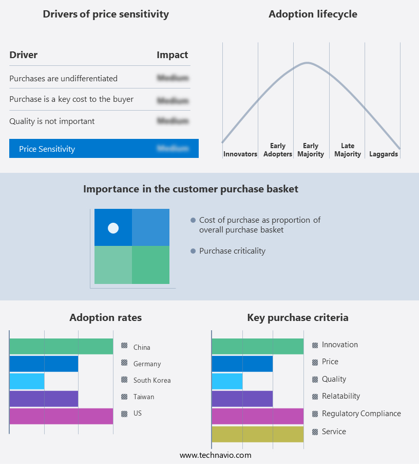
Exclusive Customer Landscape
The semiconductor glass wafer market forecasting report includes the adoption lifecycle of the market, covering from the innovator's stage to the laggard's stage. It focuses on adoption rates in different regions based on penetration. Furthermore, the semiconductor glass wafer market report also includes key purchase criteria and drivers of price sensitivity to help companies evaluate and develop their market growth analysis strategies.
Customer Landscape
Key Companies & Market Insights
Companies are implementing various strategies, such as strategic alliances, semiconductor glass wafer market forecast, partnerships, mergers and acquisitions, geographical expansion, and product/service launches, to enhance their presence in the industry.
AGC Inc. - This company specializes in providing high-precision glass substrates for Micro-Electro-Mechanical Systems (MEMS) and semiconductor packaging applications.
The industry research and growth report includes detailed analyses of the competitive landscape of the market and information about key companies, including:
- AGC Inc.
- BULLEN ULTRASONICS
- Coresix Precision Glass Inc.
- Corning Inc.
- HOYA CANDEO OPTRONICS CORP.
- Mosaic Microsystems
- Nano Quarz Wafer
- Nippon Electric Glass Co. Ltd.
- Plan Optik AG
- SCHOTT AG
- Shin Etsu Chemical Co. Ltd.
- Specialty Glass Products
- Sumitomo Electric Industries Ltd.
- Swift Glass Co Inc.
- Sydor Optics
- TECNISCO LTD.
Qualitative and quantitative analysis of companies has been conducted to help clients understand the wider business environment as well as the strengths and weaknesses of key industry players. Data is qualitatively analyzed to categorize companies as pure play, category-focused, industry-focused, and diversified; it is quantitatively analyzed to categorize companies as dominant, leading, strong, tentative, and weak.
Recent Development and News in Semiconductor Glass Wafer Market
- In February 2023, GlobalWafers, a leading semiconductor wafer manufacturer, announced the completion of its acquisition of Siltronic AG, a German wafer producer, for approximately â¬2.5 billion. This strategic move aimed to strengthen GlobalWafers' global presence and enhance its product offerings (GlobalWafers press release).
- In August 2022, Intel and Samsung Electronics formed a long-term partnership to co-develop advanced semiconductor technology, including the production of 3nm process nodes using silicon carbide and gallium nitride wafers. This collaboration is expected to accelerate the development of next-generation semiconductors and reduce production costs (Intel press release).
- In March 2021, Corning, a leading glass manufacturer, unveiled its new Gorilla Glass Victus, which is designed specifically for use in semiconductor applications. This advanced glass offers improved damage resistance and durability, making it an ideal choice for high-performance semiconductor devices (Corning press release).
- In January 2020, the European Union announced a â¬13 billion investment in the European Chip Alliance, a public-private partnership aimed at boosting Europe's semiconductor industry and reducing its reliance on imports. This initiative includes the development of advanced semiconductor technologies and the production of silicon and glass wafers (European Commission press release).
Research Analyst Overview
The market continues to evolve, driven by the constant demand for advanced technology and innovation in the semiconductor industry. Wafer standards, such as thermal stability, supply chain, doping, resistivity, cleaning, and research, play a crucial role in the production of high-quality silicon wafers. Wafer properties, including microstructure, crystallographic orientation, thickness, characterization, processing, diameter, and optical properties, are meticulously controlled to ensure optimal wafer performance. Thin film deposition, development, and wafer technology advancements continue to shape the market landscape. Wafer yield and reliability are paramount, with wafer fabrication processes focusing on minimizing defects and enhancing uniformity. Wafer packaging, handling, and storage are also essential components of the semiconductor manufacturing process.
The Semiconductor Glass Wafer Market is expanding with advancements in wafer inspection and precision-driven wafer dicing techniques. Enhanced wafer handling processes ensure improved wafer uniformity, wafer flatness, and optimized wafer resistivity for high-performance applications. The importance of wafer orientation and wafer crystallographic orientation remains critical for chip fabrication, influencing wafer conductivity and wafer chemical properties. As manufacturers focus on refining wafer microstructure, innovations extend wafer lifetime through superior durability. Ongoing wafer innovation drives technological progress, ensuring semiconductor glass wafers meet increasing industry demands.
Wafer mechanical strength, conductivity, flatness, and surface roughness are critical factors in the production of high-performance semiconductor devices. Wafer stress and lifetime are also essential considerations, with ongoing research and development efforts aimed at improving these properties. The semiconductor industry's continuous pursuit of innovation and miniaturization drives the demand for advanced wafer technologies. Glass substrates, bonding, and inspection techniques are continually evolving to meet the demands of this dynamic market. The wafer market's ongoing evolution reflects the industry's commitment to pushing the boundaries of technology and delivering superior semiconductor solutions.
The Semiconductor Glass Wafer Market is advancing with innovations in alkali-aluminosilicate glass and quartz glass, enhancing durability and performance. Materials like low-k dielectric and high-k dielectric optimize electrical properties for next-generation chips. The development of ultrathin glass and nanostructured glass enables miniaturization and improved efficiency in semiconductor fabrication. Emerging doped glass and oxide glass compositions refine functionality for specialized applications. The integration of amorphous silicon enhances conductivity and device performance. Advances in wafer metrology ensure precise quality assessment and defect detection, driving higher yields and reliability.
Dive into Technavio's strong research methodology, blending expert interviews, extensive data synthesis, and validated models for unparalleled Semiconductor Glass Wafer Market insights. See full methodology.
|
Market Scope |
|
|
Report Coverage |
Details |
|
Page number |
254 |
|
Base year |
2024 |
|
Historic period |
2019-2023 |
|
Forecast period |
2025-2029 |
|
Growth momentum & CAGR |
Accelerate at a CAGR of 4.6% |
|
Market growth 2025-2029 |
USD 174.2 million |
|
Market structure |
Fragmented |
|
YoY growth 2024-2025(%) |
4.3 |
|
Key countries |
US, China, Taiwan, South Korea, Germany, Canada, UK, India, France, and Brazil |
|
Competitive landscape |
Leading Companies, Market Positioning of Companies, Competitive Strategies, and Industry Risks |
What are the Key Data Covered in this Semiconductor Glass Wafer Market Research and Growth Report?
- CAGR of the Semiconductor Glass Wafer industry during the forecast period
- Detailed information on factors that will drive the growth and forecasting between 2025 and 2029
- Precise estimation of the size of the market and its contribution of the industry in focus to the parent market
- Accurate predictions about upcoming growth and trends and changes in consumer behaviour
- Growth of the market across APAC, North America, Europe, South America, and Middle East and Africa
- Thorough analysis of the market's competitive landscape and detailed information about companies
- Comprehensive analysis of factors that will challenge the semiconductor glass wafer market growth of industry companies
We can help! Our analysts can customize this semiconductor glass wafer market research report to meet your requirements.
 RIA -
RIA - 
