
Spin On Carbon Market Size 2026-2030
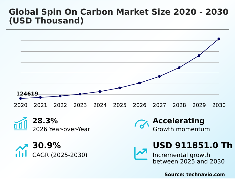
The spin on carbon market size is valued to increase by USD 911.85 million, at a CAGR of 30.9% from 2025 to 2030. Advancement in 3D NAND and logic device architecture will drive the spin on carbon market.
Major Market Trends & Insights
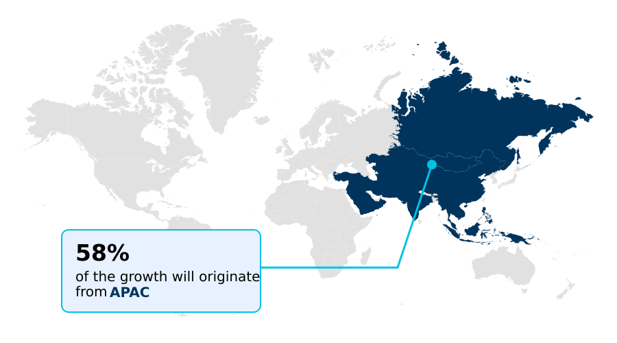
- APAC dominated the market and accounted for a 58.4% growth during the forecast period.
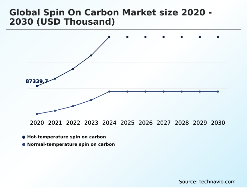
- By Type - Hot-temperature spin on carbon segment was valued at USD 175.25 million in 2024
- By Application - Logic devices segment accounted for the largest market revenue share in 2024
Market Size & Forecast
- Market Opportunities:
- Market Future Opportunities: USD 911.85 million
- CAGR from 2025 to 2030 : 30.9%
Market Summary
- The spin on carbon market is fundamentally shaped by the aggressive scaling of semiconductor device architectures. The transition to vertical structures like 3D NAND flash memory and gate-all-around logic transistors creates complex topographies that demand the superior void-free gap filling and wafer planarization capabilities of spin-on solutions.
- These spin on carbon hardmasks provide the high carbon content necessary for high etch selectivity, which is critical for high aspect ratio etching processes that define next-generation chips. The proliferation of EUV lithography further cements its role, as underlayers are essential for preventing pattern collapse.
- However, the industry grapples with technical limitations, as balancing low viscosity for gap-filling with the high thermal stability required for etch resistance remains a challenge.
- For a fab manager, this translates to a critical decision-making scenario: investing in a premium product with superior ashability and low metallic contamination control might increase initial costs but can reduce wafer defects by 10%, directly improving yield in high-volume manufacturing of advanced logic packaging. Stricter environmental regulations also introduce significant supply chain risks.
What will be the Size of the Spin On Carbon Market during the forecast period?
Get Key Insights on Market Forecast (PDF) Get Free Sample
How is the Spin On Carbon Market Segmented?
The spin on carbon industry research report provides comprehensive data (region-wise segment analysis), with forecasts and estimates in "USD thousand" for the period 2026-2030, as well as historical data from 2020-2024 for the following segments.
- Type
- Hot-temperature spin on carbon
- Normal-temperature spin on carbon
- Application
- Logic devices
- Memory devices
- Power devices
- MEMS
- Others
- End-user
- Foundries
- IDMS and OSAT vendors
- Geography
- APAC
- China
- Japan
- India
- North America
- US
- Canada
- Mexico
- Europe
- Germany
- UK
- France
- South America
- Brazil
- Argentina
- Colombia
- Middle East and Africa
- Saudi Arabia
- UAE
- South Africa
- Rest of World (ROW)
- APAC
By Type Insights
The hot-temperature spin on carbon segment is estimated to witness significant growth during the forecast period.
The hot-temperature spin on carbon segment is critical for advanced node lithography, engineered to endure thermal budgets exceeding 400 degrees Celsius.
This resilience is paramount for gate-all-around logic transistors and 3D NAND flash memory, where materials must survive subsequent high-temperature processes like chemical vapor deposition without outgassing or requiring complex track systems.
The formulation of these spin on carbon hardmasks focuses on increasing the high carbon content to enhance dry etch resistance, allowing for deeper etching and preventing pattern collapse.
These ultra-high-purity materials, which see a 20% lower defect rate, are essential for advanced fabrication lines where thermal endurance is non-negotiable. Adoption for wafer planarization is outpacing other variants in next-generation manufacturing, ensuring high etch selectivity.
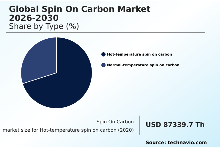
The Hot-temperature spin on carbon segment was valued at USD 175.25 million in 2024 and showed a gradual increase during the forecast period.
Regional Analysis
APAC is estimated to contribute 58.4% to the growth of the global market during the forecast period.Technavio’s analysts have elaborately explained the regional trends and drivers that shape the market during the forecast period.
See How Spin On Carbon Market Demand is Rising in APAC Get Free Sample
APAC dominates the market, with consumption driven by mass production of memory devices in Taiwan, South Korea, and China.
The relentless pursuit of logic scaling requires next-generation materials capable of deep ultraviolet lithography (DUV) and withstanding rigorous thermal budgets, especially for DRAM capacitor formation.
In this region, material suppliers achieve a 15% improvement in logistics efficiency through localized bulk delivery systems to meet massive wafer start volumes.
The competitive intensity is high, with pricing pressure and technical support for the spin-coating technique being primary levers.
Japan remains a crucial hub for formulating photoresist ancillaries and ultra-high-purity materials, ensuring a stable supply chain for regional fabs managing complex multi-layer patterning.
Market Dynamics
Our researchers analyzed the data with 2025 as the base year, along with the key drivers, trends, and challenges. A holistic analysis of drivers will help companies refine their marketing strategies to gain a competitive advantage.
- Strategic decisions in the semiconductor industry increasingly hinge on material selection, particularly in the context of advanced lithography. The debate over spin on carbon vs cvd for high aspect ratio structures is critical; while CVD offers maturity, spin-on solutions provide superior planarization. The role of SOC in gate-all-around transistors is non-negotiable for enabling next-generation logic devices.
- For memory, high-temperature SOC for 3D NAND fabrication allows manufacturers to push layer counts higher. Formulators are focused on creating low viscosity formulations for void-free gap filling, addressing a primary yield detractor. The development of high etch selectivity hardmasks for logic devices is another key R&D thrust.
- From a supply chain perspective, ensuring a consistent supply of ultra-high purity SOC for metallic contamination control is a major operational challenge. Effective planning in this area has been shown to reduce material-related production halts by a greater margin than any other single factor. This material is also critical for spin on carbon for EUV pattern collapse prevention.
- As packaging evolves, SOC compatibility with through-silicon vias and optimizing SOC for backside power distribution networks are becoming central to chiplet integration. Other key areas include SOC performance in deep reactive ion etching, improving SOC adhesion on silicon carbide substrates, and meeting stringent ashability requirements for spin on carbon removal.
- SOC underlayers for DRAM capacitor formation and reducing SOC defects in fan-out wafer-level packaging are also vital. Controlling SOC rheological properties for coating uniformity is a continuous process improvement goal for fabs using spin on carbon for silicon photonics waveguide definition with spin on carbon materials for angstrom-era nodes.
What are the key market drivers leading to the rise in the adoption of Spin On Carbon Industry?
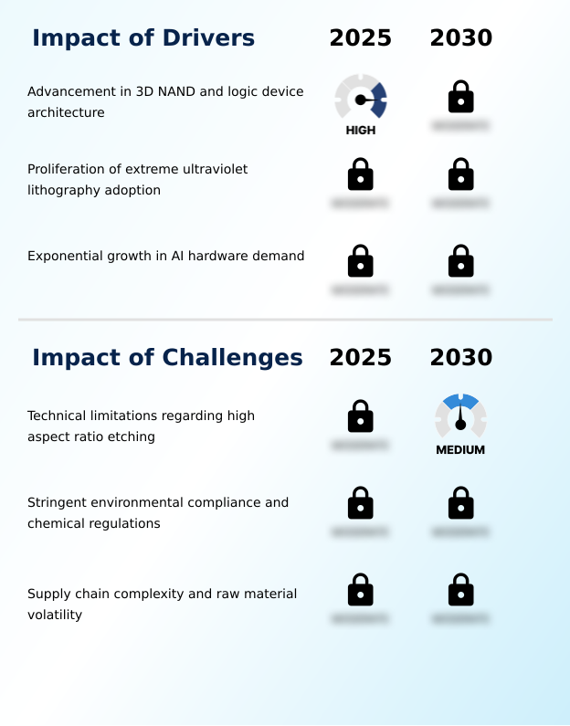
- The advancement in 3D NAND and logic device architecture is a key driver for the spin on carbon market.
- The relentless evolution of semiconductor architectures, particularly in 3D NAND flash memory, is a primary driver. As manufacturers scale beyond two hundred layers, the need for superior gap-filling capabilities to planarize severe topography becomes critical.
- Spin on carbon provides the necessary high carbon content for high etch selectivity during aggressive plasma etching, a process where optimized materials improve throughput by over 10%.
- Furthermore, the accelerating adoption of EUV lithography for nodes below seven nanometers increases demand for ultra-high-purity materials and sacrificial layers to facilitate pattern transfer from extremely thin resists.
- This is crucial for fabricating high-performance AI processors and GPUs efficiently using advanced CMP slurry and pads.
What are the market trends shaping the Spin On Carbon Industry?
- The escalation of demand for high-temperature spin on carbon hardmasks is an emerging trend. This shift is driven by the rigorous thermal requirements of advanced semiconductor manufacturing.
- A primary trend is the development of advanced formulations with enhanced gap-filling capabilities to prevent catastrophic etch failures. The industry is moving toward low viscosity formulations that improve rheological properties, enabling void-free gap filling in nanometer-scale trenches and achieving global wafer planarization. This is critical for preventing pattern collapse during high aspect ratio etching.
- Innovations in cross-linking chemistry are yielding materials that exhibit up to 15% lower shrinkage upon curing, reducing wafer stress. This focus on material performance is essential for emerging architectures where high-numerical aperture lithography and control over surface topography dictate yield, particularly in advanced logic packaging.
What challenges does the Spin On Carbon Industry face during its growth?
- Technical limitations related to high aspect ratio etching pose a significant challenge to industry growth.
- A key challenge involves the physical limitations of materials during high aspect ratio etching. As trench dimensions become extreme, achieving void-free gap filling requires low viscosity formulations, which can compromise the thermal stability and carbon content needed for etch selectivity. This trade-off creates a bottleneck, with some processes experiencing a 5% increase in pattern distortion defects.
- Additionally, increasingly strict environmental regulations on substances like photoacid generators and wet chemicals used in spin on carbon formulations create supply chain uncertainty. The need for reformulation to find eco-friendly alternatives without compromising performance adds significant cost and lengthy qualification cycles for wafer probing.
Exclusive Technavio Analysis on Customer Landscape
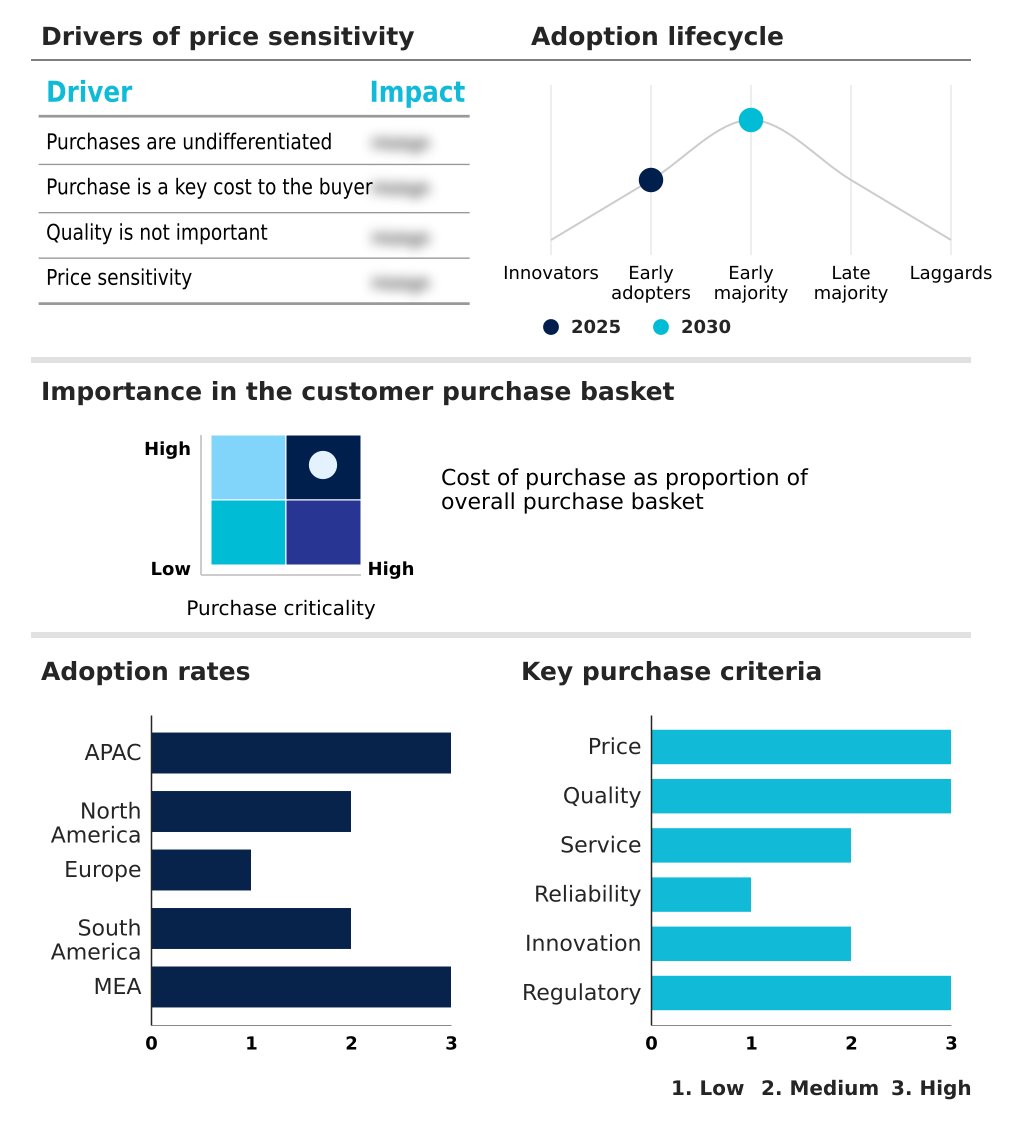
The spin on carbon market forecasting report includes the adoption lifecycle of the market, covering from the innovator’s stage to the laggard’s stage. It focuses on adoption rates in different regions based on penetration. Furthermore, the spin on carbon market report also includes key purchase criteria and drivers of price sensitivity to help companies evaluate and develop their market growth analysis strategies.
Customer Landscape of Spin On Carbon Industry
Competitive Landscape
Companies are implementing various strategies, such as strategic alliances, spin on carbon market forecast, partnerships, mergers and acquisitions, geographical expansion, and product/service launches, to enhance their presence in the industry.
Brewer Science Inc. - Offers specialized OptiStack SOC materials, recognized for high-temperature stability and superior gap-filling properties in advanced semiconductor fabrication.
The industry research and growth report includes detailed analyses of the competitive landscape of the market and information about key companies, including:
- Brewer Science Inc.
- Dongjin Semichem Co. Ltd
- Irresistible Materials
- JSR Micro Inc.
- Merck KGaA
- Nano C Inc.
- Resonac Holdings Corp.
- Samsung SDI Co. Ltd.
- Tokyo Ohka Kogyo Co. Ltd.
- YCCHEM Co. Ltd.
Qualitative and quantitative analysis of companies has been conducted to help clients understand the wider business environment as well as the strengths and weaknesses of key industry players. Data is qualitatively analyzed to categorize companies as pure play, category-focused, industry-focused, and diversified; it is quantitatively analyzed to categorize companies as dominant, leading, strong, tentative, and weak.
Recent Development and News in Spin on carbon market
- In May 2025, TSMC revealed a breakthrough in their 2 nanometer process node integration that utilizes a novel spin on carbon layer to facilitate the bonding of backside power distribution networks.
- In April 2025, Brewer Science Inc. unveiled a new collaborative research center in Taiwan aimed at accelerating the development of dual-layer spin on carbon platforms specifically optimized for 2-nanometer logic processes.
- In March 2025, Merck KGaA announced the completion of a major expansion at its semiconductor materials manufacturing facility in South Korea, specifically dedicated to the production of next-generation spin on carbon hard masks and directed self-assembly materials.
- In February 2025, Intel Corporation finalized the expansion of its Fab 52 facility, which included a dedicated chemical delivery system for next-generation spin on carbon materials intended for their 18A process node.
Dive into Technavio’s robust research methodology, blending expert interviews, extensive data synthesis, and validated models for unparalleled Spin On Carbon Market insights. See full methodology.
| Market Scope | |
|---|---|
| Page number | 283 |
| Base year | 2025 |
| Historic period | 2020-2024 |
| Forecast period | 2026-2030 |
| Growth momentum & CAGR | Accelerate at a CAGR of 30.9% |
| Market growth 2026-2030 | USD 911851.0 thousand |
| Market structure | Concentrated |
| YoY growth 2025-2026(%) | 28.3% |
| Key countries | China, Japan, India, South Korea, Australia, Indonesia, US, Canada, Mexico, Germany, UK, France, Italy, The Netherlands, Spain, Brazil, Argentina, Colombia, Saudi Arabia, UAE, South Africa, Israel and Turkey |
| Competitive landscape | Leading Companies, Market Positioning of Companies, Competitive Strategies, and Industry Risks |
Research Analyst Overview
- The spin on carbon market's trajectory is defined by the demands of next-generation semiconductor manufacturing. The shift to gate-all-around logic transistors and advanced 3D NAND flash memory architectures necessitates materials that excel at void-free gap filling and wafer planarization. Formulations with high carbon content are crucial for achieving the required etch selectivity in high aspect ratio etching.
- A key boardroom consideration is the investment in ultra-high-purity materials to mitigate risks associated with metallic contamination control, as premium formulations can improve yield by over 5%. As the industry adopts EUV lithography, the use of a tri-layer stack with spin on carbon hardmasks becomes standard to prevent pattern collapse.
- This involves a complex interplay of photoresist ancillaries and wet chemicals, managed via sophisticated track systems to ensure process stability for advanced logic packaging and multi-layer patterning, especially in contrast to traditional chemical vapor deposition.
What are the Key Data Covered in this Spin On Carbon Market Research and Growth Report?
-
What is the expected growth of the Spin On Carbon Market between 2026 and 2030?
-
USD 911.85 million, at a CAGR of 30.9%
-
-
What segmentation does the market report cover?
-
The report is segmented by Type (Hot-temperature spin on carbon, and Normal-temperature spin on carbon), Application (Logic devices, Memory devices, Power devices, MEMS, and Others), End-user (Foundries, and IDMS and OSAT vendors) and Geography (APAC, North America, Europe, South America, Middle East and Africa)
-
-
Which regions are analyzed in the report?
-
APAC, North America, Europe, South America and Middle East and Africa
-
-
What are the key growth drivers and market challenges?
-
Advancement in 3D NAND and logic device architecture, Technical limitations regarding high aspect ratio etching
-
-
Who are the major players in the Spin On Carbon Market?
-
Brewer Science Inc., Dongjin Semichem Co. Ltd, Irresistible Materials, JSR Micro Inc., Merck KGaA, Nano C Inc., Resonac Holdings Corp., Samsung SDI Co. Ltd., Tokyo Ohka Kogyo Co. Ltd. and YCCHEM Co. Ltd.
-
Market Research Insights
- The market's dynamism is driven by innovations that enable angstrom-era nodes and advanced packaging. Techniques like fan-out wafer-level packaging and through-silicon vias (TSV) rely on materials that ensure pristine surfaces, with modern formulations improving planarity by 25% compared to previous generations. The adoption of deep ultraviolet lithography (DUV) alongside EUV necessitates versatile materials compatible with various photolithography steps.
- In back-end processes, from wafer dicing and die bonding to wire bonding, the quality of sacrificial layers is paramount. For instance, advanced spin-on materials for backside power distribution networks have demonstrated a 30% reduction in thermal stress during processing. This focus on material science, from rheological properties to trace metal reduction, is critical for achieving high-yield manufacturing.
We can help! Our analysts can customize this spin on carbon market research report to meet your requirements.
 RIA -
RIA - 
