
Nanopatterning Market Size 2025-2029
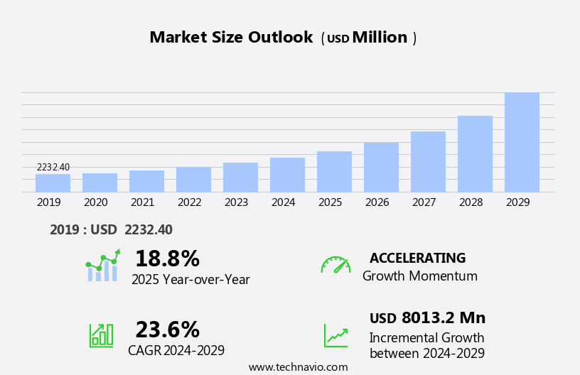
The nanopatterning market size is forecast to increase by USD 8.01 billion, at a CAGR of 23.6% between 2024 and 2029.
- The market is experiencing significant growth due to the emergence of advanced consumer products and the increasing use of semiconductor devices in automobiles. These trends are driving the demand for nanopatterning technologies, which enable the creation of intricate patterns at the nanoscale level. However, the market faces challenges, primarily the increasing cost of lithography functions, which is a critical process in nanopatterning. This cost escalation poses a significant obstacle for companies seeking to adopt nanopatterning technologies, as it can hinder their profitability and competitiveness.
- To capitalize on market opportunities and navigate these challenges effectively, companies must focus on developing cost-effective nanopatterning solutions while maintaining high performance and precision. By doing so, they can cater to the growing demand for advanced consumer products and the integration of semiconductor devices in various industries, ultimately securing a competitive edge in the market.
What will be the Size of the Nanopatterning Market during the forecast period?
Explore in-depth regional segment analysis with market size data - historical 2019-2023 and forecasts 2025-2029 - in the full report.
Request Free Sample
The market continues to evolve, driven by the ongoing quest for advanced materials and technologies. Reactive ion etching, soft lithography, physical vapor deposition, and atomic layer deposition are among the techniques used to create intricate nanostructures with precise control over aspect ratio and mechanical properties. These techniques find applications in various sectors, including biomedical applications, energy storage, and electronics. Biomedical researchers utilize nanopatterning for creating nanofluidic devices and microscale patterning for tissue engineering and drug delivery systems. In energy storage, nanoporous materials and subwavelength structures are used to enhance the performance of batteries and solar cells.
Nanopatterning techniques also play a crucial role in creating periodic structures for photonic crystals and surface plasmon resonance applications. Electrical properties, thermal properties, and optical properties are all manipulated to optimize device performance. Process control and pattern fidelity are critical considerations in nanopatterning, with plasma etching, chemical vapor deposition, and deep ultraviolet lithography used to address these challenges. Wet etching and nanoimprint lithography are also employed for pattern transfer methods. As feature sizes continue to shrink, resolution limits and the importance of nanoparticle assembly and self-assembled monolayers become increasingly relevant. The market dynamics of nanopatterning are constantly unfolding, with new techniques and applications emerging to meet the evolving demands of various industries.
How is this Nanopatterning Industry segmented?
The nanopatterning industry research report provides comprehensive data (region-wise segment analysis), with forecasts and estimates in "USD million" for the period 2025-2029, as well as historical data from 2019-2023 for the following segments.
- Product Type
- Nanoimprint
- E-beam lithography
- Others
- End-user
- IDM
- Foundry
- Geography
- North America
- US
- Canada
- Europe
- France
- Germany
- Italy
- UK
- APAC
- China
- India
- Japan
- Taiwan
- Rest of World (ROW)
- North America
.
By Product Type Insights
The nanoimprint segment is estimated to witness significant growth during the forecast period.
The market is witnessing significant growth due to the increasing demand for miniaturized devices with enhanced functionalities in various industries, including electronics, energy storage, and biomedical applications. Reactive ion etching, soft lithography, physical vapor deposition, and atomic layer deposition are among the commonly used nanopatterning techniques to achieve subwavelength structures with high aspect ratio and precise process control. These techniques enable the fabrication of nanofluidic devices, photonic crystals, and surface plasmon resonance structures, which are essential for advanced technologies such as solar cells and nanoporous materials. Electron beam lithography and nanoimprint lithography are other pattern transfer methods used to create high-resolution features with pattern fidelity.
Plasma etching and wet etching are essential process steps for dry and wet etching, respectively, to achieve the desired pattern geometry. Deep ultraviolet lithography and self-assembled monolayers are critical tools for surface modification and pattern transfer. The market trends include the development of nanoparticle assembly techniques for creating periodic structures and the integration of block copolymer self-assembly for producing complex nanostructures. The focus on improving pattern transfer methods, increasing resolution limits, and enhancing optical and thermal properties is driving the market's growth. These advancements are leading to the production of advanced devices with improved mechanical, electrical, and optical properties, making them suitable for various applications such as energy storage, biomedical devices, and photonics.
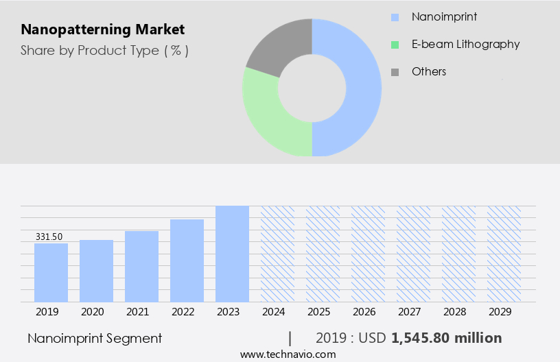
The Nanoimprint segment was valued at USD 1.55 billion in 2019 and showed a gradual increase during the forecast period.
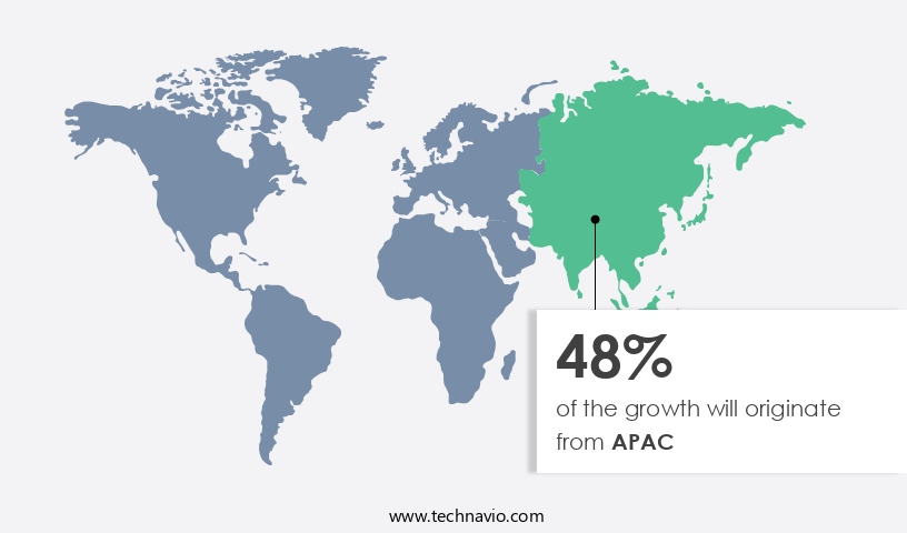
Regional Analysis
APAC is estimated to contribute 48% to the growth of the global market during the forecast period. Technavio's analysts have elaborately explained the regional trends and drivers that shape the market during the forecast period.
In the market, various techniques such as reactive ion etching, soft lithography, physical vapor deposition, and atomic layer deposition are employed to create nanoscale structures with high aspect ratio and precise mechanical properties. These techniques find extensive applications in biomedical fields, energy storage, and nanofluidic devices, among others. For instance, nanopatterning is crucial in creating subwavelength structures for photonic crystals and surface plasmon resonance, enhancing the optical properties of solar cells. Electron beam lithography and self-assembled monolayers are essential in surface modification for enhancing pattern fidelity. In the field of microscale patterning, process control is paramount, with techniques like deep ultraviolet lithography, block copolymer self-assembly, and nanoimprint lithography playing significant roles.
Dry etching and chemical vapor deposition are essential for creating periodic structures, while plasma etching and wet etching are used for pattern transfer methods. The market is driven by the increasing demand for miniaturized ICs from various industries, including aerospace and defense, automotive, Consumer Electronics, and healthcare. The demand for nanopatterning techniques is also fueled by the growing implementation of IoT, increasing automation, and investment in human-machine interface technologies. In APAC, the presence of major semiconductor foundries and consumer electronics manufacturers is creating a significant demand for nanopatterning techniques.
Market Dynamics
Our researchers analyzed the data with 2024 as the base year, along with the key drivers, trends, and challenges. A holistic analysis of drivers will help companies refine their marketing strategies to gain a competitive advantage.
What are the key market drivers leading to the rise in the adoption of Nanopatterning Industry?
- The advanced consumer products sector serves as the primary catalyst for market growth, with continuous innovation and technological advancements shaping consumer preferences and driving market expansion.
- The market is experiencing significant advancements due to the increasing demand for surface modification in various industries. Deep ultraviolet lithography and wet etching are the primary technologies used to achieve high-precision nanopatterning. The resolution limits of these techniques are continually being pushed to enable the fabrication of nanoscale features with improved optical properties. Nanoparticle assembly and nanoimprint lithography are alternative pattern transfer methods gaining popularity due to their potential for mass production and cost-effectiveness. The ability to manipulate and control nanoscale features offers numerous applications, including electronics, energy, and healthcare.
- The market's growth is driven by the increasing demand for miniaturization and the need for improved performance in various industries. The future of nanopatterning lies in the development of new technologies and the optimization of existing ones to meet the evolving demands of the market.
What are the market trends shaping the Nanopatterning Industry?
- The use of semiconductor devices in automobiles is becoming increasingly prevalent, representing a significant market trend. These advanced technologies enhance vehicle performance and functionality, contributing to the automotive industry's ongoing evolution.
- The market experiences significant growth due to the increasing demand for advanced semiconductor technologies in various industries, particularly in automotive and electronics. Semiconductor devices are integral components of numerous applications, such as car navigation and display systems, airbag management, GPS, anti-lock braking systems (ABS), power windows and doors, entertainment systems, automated driving, and collision detection technology. With the rise in automobile production, the demand for these devices is expected to surge, leading to increased production of semiconductor wafers. Consequently, nanopatterning systems are in high demand to produce the intricate patterns required for semiconductor fabrication.
- Techniques such as reactive ion etching, soft lithography, physical vapor deposition, and atomic layer deposition are essential in achieving the desired aspect ratios and mechanical properties for these applications. The market is expected to continue its growth trajectory, driven by the increasing demand for semiconductor devices and the advancements in nanotechnology.
What challenges does the Nanopatterning Industry face during its growth?
- The escalating costs of lithography functions pose a significant challenge to the growth of the industry. Lithography, an essential process in semiconductor manufacturing, is becoming increasingly expensive, threatening to hinder the industry's expansion and profitability.
- The market is experiencing significant changes due to advancements in semiconductor technology, specifically the reduction of node sizes. These technological transitions are impacting the lithography process, leading the nanopatterning industry to adopt high-resolution techniques such as double patterning and EUV lithography. While these methods increase the resolution and accuracy of patterning, they also significantly increase the cost of lithography. The cost of EUV lithography is approximately 35% higher than that of ArF immersion lithography. Consequently, the rising cost of lithography functions is expected to pose a challenge to the growth of the market. Nanopatterning techniques, including EUV lithography, are essential for creating subwavelength structures, such as nanofluidic devices, photonic crystals, and microscale patterning used in various applications, including solar cells.
- The electrical and thermal properties of these structures are critical for their performance. Plasma etching and electron beam lithography are other nanopatterning techniques used to achieve high-resolution patterning. Despite the challenges, the market is expected to continue growing due to the increasing demand for advanced technologies in various industries.
Exclusive Customer Landscape
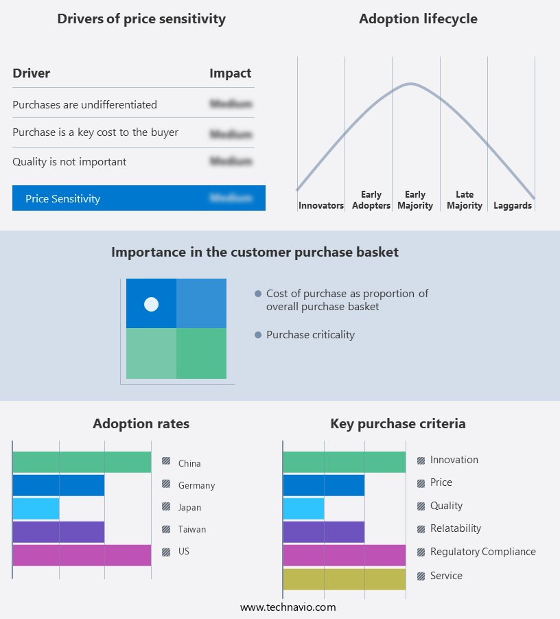
The nanopatterning market forecasting report includes the adoption lifecycle of the market, covering from the innovator's stage to the laggard's stage. It focuses on adoption rates in different regions based on penetration. Furthermore, the nanopatterning market report also includes key purchase criteria and drivers of price sensitivity to help companies evaluate and develop their market growth analysis strategies.
Customer Landscape
Key Companies & Market Insights
Companies are implementing various strategies, such as strategic alliances, nanopatterning market forecast, partnerships, mergers and acquisitions, geographical expansion, and product/service launches, to enhance their presence in the industry.
AMO GmbH - The company specializes in nanopatterning services, creating active and passive integrated nanophotonics devices.
The industry research and growth report includes detailed analyses of the competitive landscape of the market and information about key companies, including:
- AMO GmbH
- EV Group
- Fraunhofer Gesellschaft
- Institute for Microelectronics Stuttgart
- Meta Materials Inc.
- Micro resist technology GmbH
- Nanonex Corp.
- Nanoscribe GmbH and Co. KG
- Nanotypos
- NIL Technology ApS
- Nippon Telegraph and Telephone Corp.
- Obducat AB
- Raith GmbH
- SET Corp SA
- SUSS MICROTEC SE
- SVG Optronics Co. Ltd.
- Toppan Inc.
- Transfer Devices Inc.
- Upper Austrian Research GmbH
- Vistec Electron Beam GmbH
Qualitative and quantitative analysis of companies has been conducted to help clients understand the wider business environment as well as the strengths and weaknesses of key industry players. Data is qualitatively analyzed to categorize companies as pure play, category-focused, industry-focused, and diversified; it is quantitatively analyzed to categorize companies as dominant, leading, strong, tentative, and weak.
Recent Development and News in Nanopatterning Market
- In February 2024, Intel Corporation unveiled its new Intel PentoniQ technology, which utilizes advanced nanopatterning techniques for manufacturing transistors with high precision and density. This development marks a significant stride towards the realization of Intel's 7nm and beyond technology nodes (Intel Press Release, 2024).
- In May 2024, ASML Holding NV, a leading provider of photolithography equipment, announced a strategic collaboration with Tokyo Electron Limited to jointly develop extreme ultraviolet (EUV) lithography systems for the mass production of semiconductors using nanopatterning technology. This partnership is expected to accelerate the adoption of EUV lithography and reduce the manufacturing costs for the semiconductor industry (ASML Press Release, 2024).
- In August 2024, Nanomix, a nanopatterning technology company, secured a USD 30 million Series C funding round led by New Enterprise Associates and 8VC. The funds will be used to scale up production and expand the company's customer base in the biotech and pharmaceutical industries (Nanomix Press Release, 2024).
Research Analyst Overview
- The market encompasses various applications, including surface engineering for wear resistance and corrosion resistance, anti-fouling coatings, and the development of next-generation materials. Thin film deposition techniques, such as atomic force microscopy (AFM) and scanning electron microscopy (SEM), play a crucial role in achieving feature definition at the nanoscale. Hybrid materials and bio-inspired materials are gaining popularity due to their functional properties, leading to advancements in responsive materials and smart materials. Pattern generation and transfer methods, including optical microscopy and etching techniques, are essential for creating intricate patterns on surfaces. Nanoscale characterization tools, such as contact angle measurements, X-ray diffraction, and AFM, enable accurate analysis of material properties.
- Deposition techniques like pattern replication and surface texturing are vital for enhancing surface roughness and contact angle, contributing to the market's growth. Smart materials with unique properties, such as self-healing and shape memory, are driving innovation in various industries. Overall, the market is witnessing significant advancements in the development and application of advanced materials, pattern generation, and surface analysis techniques.
Dive into Technavio's robust research methodology, blending expert interviews, extensive data synthesis, and validated models for unparalleled Nanopatterning Market insights. See full methodology.
|
Market Scope |
|
|
Report Coverage |
Details |
|
Page number |
199 |
|
Base year |
2024 |
|
Historic period |
2019-2023 |
|
Forecast period |
2025-2029 |
|
Growth momentum & CAGR |
Accelerate at a CAGR of 23.6% |
|
Market growth 2025-2029 |
USD 8013.2 million |
|
Market structure |
Fragmented |
|
YoY growth 2024-2025(%) |
18.8 |
|
Key countries |
US, Taiwan, China, Japan, India, Germany, Canada, UK, France, and Italy |
|
Competitive landscape |
Leading Companies, Market Positioning of Companies, Competitive Strategies, and Industry Risks |
What are the Key Data Covered in this Nanopatterning Market Research and Growth Report?
- CAGR of the Nanopatterning industry during the forecast period
- Detailed information on factors that will drive the growth and forecasting between 2025 and 2029
- Precise estimation of the size of the market and its contribution of the industry in focus to the parent market
- Accurate predictions about upcoming growth and trends and changes in consumer behaviour
- Growth of the market across APAC, North America, Europe, South America, and Middle East and Africa
- Thorough analysis of the market's competitive landscape and detailed information about companies
- Comprehensive analysis of factors that will challenge the nanopatterning market growth of industry companies
We can help! Our analysts can customize this nanopatterning market research report to meet your requirements.
 RIA -
RIA - 
