Semiconductor Assembly And Packaging Services Market Size 2024-2028
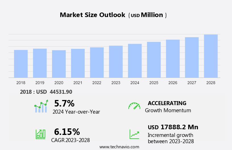
The semiconductor assembly and packaging services market size is forecast to increase by USD 17.89 billion, at a CAGR of 6.15% between 2023 and 2028.
- The market is experiencing significant growth due to the increasing demand for semiconductor wafers and the short product lifecycle of mobile devices. The need for high initial capital investments is a challenge for market participants. The market trends reflect the continuous advancements in semiconductor technology and miniaturization, leading to the production of smaller, more efficient, and high-performance devices. The growing adoption of the Internet of Things and automotive applications is further fueling the market's growth. Despite these opportunities, the market faces challenges such as the high cost of manufacturing and the need for continuous innovation to keep up with the rapidly evolving technology landscape. Overall, the market is expected to witness steady growth in the coming years, driven by these trends and challenges.
What will be the Size of the Semiconductor Assembly And Packaging Services Market During the Forecast Period?
- The market encompasses the processes involved in transforming integrated circuits (ICs) from raw wafers into finished semiconductor components. This market caters to various packaging technologies, including surface mount technology (SMT) for ball grid array (BGA) and flip chip, as well as wire bonding and die attach for wafer bumping. Advanced packaging techniques, such as 3D IC, substrate, leadframe, and encapsulation, are also part of this market's scope. Semiconductor foundries and outsourced semiconductor assembly and testing (OSAT) companies provide these services to the electronics industry, enabling the production of complex microelectronic devices, including MEMS packaging and microelectronics. Market dynamics are influenced by factors such as increasing demand for miniaturization, higher performance, and lower power consumption in electronic devices. These trends drive the adoption of advanced packaging solutions, pushing the market towards continuous innovation and growth.
How is this Semiconductor Assembly And Packaging Services Industry segmented and which is the largest segment?
The semiconductor assembly and packaging services industry research report provides comprehensive data (region-wise segment analysis), with forecasts and estimates in "USD billion" for the period 2024-2028, as well as historical data from 2018-2022 for the following segments.
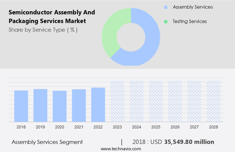
- Service Type
- Assembly services
- Testing services
- Application
- Communication
- Computing and networking
- Industrial
- Consumer electronics
- Automotive electronics
- Geography
- APAC
- China
- Japan
- South Korea
- North America
- US
- Europe
- South America
- Middle East and Africa
- APAC
By Service Type Insights
- The assembly services segment is estimated to witness significant growth during the forecast period.
The market encompasses various processes, including chip packaging, die attach, wire bonding, encapsulation, testing services, backend processing, and frontend processing. Technologies such as ball grid array (BGA), flip chip, wafer bumping, 3D IC, and chip-scale packaging (CSP) are commonly used. WLP, particularly fan-out wafer-level packaging (FOWLP and FIWLP), is popular for manufacturing integrated circuits (ICs), especially for analog, linear, and passive components. Market participants aim to reduce costs and simplify technology to cater to original equipment manufacturers (OEMs). IC demand is influenced by consumer electronic goods segments, making it crucial for semiconductor assembly and packaging services.
Get a glance at the Semiconductor Assembly And Packaging Services Industry report of share of various segments Request Free Sample
The assembly services segment was valued at USD 35.55 billion in 2018 and showed a gradual increase during the forecast period.
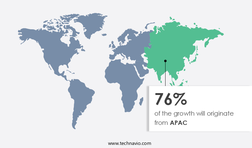
Regional Analysis
- APAC is estimated to contribute 76% to the growth of the global market during the forecast period.
Technavio's analysts have elaborately explained the regional trends and drivers that shape the market during the forecast period.
For more insights on the market share of various regions, Request Free Sample
The market in APAC is fueled by the presence of leading semiconductor foundries, including TSMC, United Microelectronics, Samsung, and Semiconductor Manufacturing International. These companies are expanding their operations in the region by constructing new fabrication units. China, with supportive government policies, is also planning to establish new production facilities. Semiconductor manufacturing powerhouses in countries like Taiwan, Japan, and South Korea require assembly and packaging services, contributing to market growth. companies such as SPIL and ASE provide back-end processing support to major foundries like TSMC and UMC.
Integrated circuits (ICs) go through various processes, including chip packaging (SiP, Ball Grid Array, Flip Chip), wafer bumping (3D IC, Die Attach), wire bonding, encapsulation, testing services, and backend processing (frontend processing, substrate, leadframe). Advanced packaging technologies, such as thermal management, reliability testing, SMT, thin film technology, and photonics packaging, are also part of the semiconductor assembly and packaging services landscape. Packaging materials, including silicon wafers and wafer fabrication, are essential components of this market.
Market Dynamics
Our researchers analyzed the data with 2023 as the base year, along with the key drivers, trends, and challenges. A holistic analysis of drivers will help companies refine their marketing strategies to gain a competitive advantage.
What are the key market drivers leading to the rise in the adoption of Semiconductor Assembly And Packaging Services Industry?
Growing demand for semiconductor wafers is the key driver of the market.
- The market is experiencing significant growth, driven by the increasing demand for integrated circuits (ICs) and advanced packaging technologies such as Chip Scale Packaging (CSP), Ball Grid Array (BGA), Flip Chip, and System in Package (SiP). Semiconductor foundries, Original Equipment Manufacturers (OEMs), and Outsourced Semiconductor Assembly and Testing (OSAT) companies are key players in this market. Semiconductor assembly and packaging services include processes such as die attach, wire bonding, encapsulation, testing services, and backend processing. Thermal management and reliability testing are crucial aspects of semiconductor packaging to ensure the longevity and performance of the devices. The market for semiconductor packaging materials, including substrates, leadframes, and packaging materials, is also growing in parallel with the semiconductor industry.
- Advanced packaging technologies, such as 3D IC, thin film technology, MEMS packaging, photonics packaging, RFID, and wafer fabrication, are gaining popularity due to their ability to increase device performance and functionality. The semiconductor industry is witnessing a ruse in demand for semiconductor devices in various applications, including consumer electronics, automotive, industrial, and telecommunications. The increasing adoption of microelectronics in these industries is fueling the growth of the market. Semiconductor wafer dicing, wafer bumping, and chip-scale packaging are essential processes in semiconductor manufacturing, and they are critical to the overall success of the semiconductor industry. The market for these services is expected to grow at a CAGR of 6.5%
- during the forecast period. The market is a complex and dynamic industry that requires a high level of expertise and technology. Companies offering these services must stay up-to-date with the latest technologies and trends to remain competitive. The market is expected to continue its growth trajectory, driven by the increasing demand for semiconductor devices and the development of new packaging technologies.
What are the market trends shaping the Semiconductor Assembly And Packaging Services Industry?
The short product lifecycle of mobile devices is the upcoming market trend.
- The market encompasses a range of integrated circuit (IC) processing techniques, including chip packaging, SiP, Ball Grid Array (BGA), Flip Chip, Wafer Bumping, 3D IC, Die Attach, Wire Bonding, Encapsulation, Testing Services, Backend Processing, Frontend Processing, Substrate, Leadframe, and various advanced packaging technologies. These services are essential for the production of microelectronics, MEMS, photonics, RFID, and other electronic packaging applications. Key processes in semiconductor assembly and packaging include wafer dicing, chip-scale packaging (CSP), Quad Flat Package (QFP), and thin film technology. Wafer fabrication and packaging materials are crucial components of these services. The market is driven by the increasing demand for advanced electronic devices, such as smartphones, computers, and automotive electronics.
- The need for high-performance, compact, and energy-efficient devices is pushing the boundaries of semiconductor technology and packaging techniques. Testing services, including thermal management and reliability testing, are crucial to ensure the quality and durability of semiconductor devices. Semiconductor foundries, OSATs, and IDMs rely on these services to meet the growing demand for electronic components in various industries. The market is expected to grow significantly due to the increasing adoption of advanced packaging technologies, such as 3D IC, SiP, and flip chip, which offer higher performance, lower power consumption, and smaller form factors. In summary, the market is a dynamic and evolving industry that plays a vital role in the production of advanced electronic devices.
What challenges does the Semiconductor Assembly And Packaging Services Industry face during its growth?
The need for high initial capital investments is a key challenge affecting the industry growth.
- The semiconductor industry is undergoing significant transformations with the increasing demand for compact Integrated Circuits (ICs) and the emergence of advanced packaging solutions. Semiconductor companies face the challenge of aligning manufacturing processes with new packaging technologies, leading to increased ownership and maintenance costs. To mitigate this, many device manufacturers outsource the manufacturing and packaging of their ICs to Semiconductor Foundries and Outsourced Semiconductor Assembly and Testing (OSAT) services such as TSMC and ASE. Advanced packaging solutions like 3D ICs, SiP, Ball Grid Array (BGA), Flip Chip, Wafer Bumping, and Chip-Scale Packaging (CSP) have revolutionized the semiconductor industry. Technologies like Thin Film Technology, Wire Bonding, Die Attach, Encapsulation, and Testing Services are crucial in the backend processing of ICs.
- Substrate materials like Silicon Wafer, Leadframe, and Packaging Materials play a vital role in the frontend processing. The semiconductor industry also caters to various applications, including MEMS Packaging, Microelectronics, Photonics Packaging, RFID, and Wafer Fabrication. Advanced packaging solutions like 3D ICs, Thermal Management, and Reliability Testing are essential for the manufacturing of these applications. SMT, Bumping Services, Wafer Dicing, and Quad Flat Package (QFP) are some of the other critical processes in the market. The market is a complex ecosystem that requires significant capital investment for manufacturing setup. Companies with low-scale production of ICs opt to outsource the manufacturing and packaging processes to specialized foundries and OSATs to reduce costs and focus on their core competencies.
Exclusive Customer Landscape
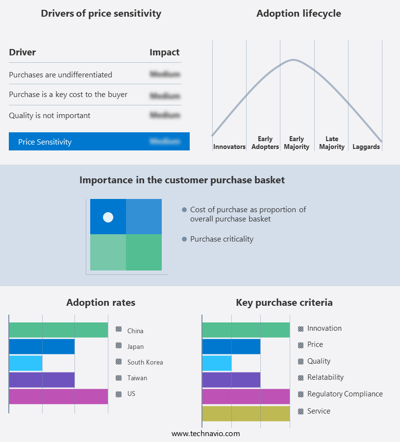
The semiconductor assembly and packaging services market forecasting report includes the adoption lifecycle of the market, covering from the innovator's stage to the laggard's stage. It focuses on adoption rates in different regions based on penetration. Furthermore, the semiconductor assembly and packaging services market report also includes key purchase criteria and drivers of price sensitivity to help companies evaluate and develop their market growth analysis strategies.
Customer Landscape
Key Companies & Market Insights
Companies are implementing various strategies, such as strategic alliances, semiconductor assembly and packaging services market forecast, partnerships, mergers and acquisitions, geographical expansion, and product/service launches, to enhance their presence in the industry.
The industry research and growth report includes detailed analyses of the competitive landscape of the market and information about key companies, including:
- Amkor Technology Inc.
- ASE Technology Holding Co. Ltd.
- ASMPT Ltd.
- ChipMOS TECHNOLOGIES INC.
- HANA Micron Co. Ltd.
- Intel Corp.
- Jiangsu Changdian Technology Co. Ltd.
- King Yuan Electronics Co. Ltd.
- KLA Corp.
- Microchip Technology Inc.
- Powertech Technology Inc.
- Promex Industries Inc.
- Renesas Electronics Corp.
- Samsung Electronics Co. Ltd.
- SIGNETICS Corp.
- Taiwan Semiconductor Manufacturing Co. Ltd.
- Tokyo Electron Ltd.
- Toshiba Corp.
- ULVAC Inc.
- Yole Developpement SA
Qualitative and quantitative analysis of companies has been conducted to help clients understand the wider business environment as well as the strengths and weaknesses of key industry players. Data is qualitatively analyzed to categorize companies as pure play, category-focused, industry-focused, and diversified; it is quantitatively analyzed to categorize companies as dominant, leading, strong, tentative, and weak.
Research Analyst Overview
Semiconductor assembly and packaging services play a crucial role in the production of integrated circuits (ICs), also known as chips. These services encompass various processes that transform raw silicon wafers into functional electronic components. The semiconductor industry relies heavily on these services to ensure the efficient and reliable manufacturing of ICs. The semiconductor assembly process involves several steps, including die attach, wire bonding, and encapsulation. Die attach is the process of attaching the IC die to a substrate or leadframe using adhesives or other bonding materials. Wire bonding is the method of connecting the die to the external circuitry using ultra-fine wires.
Further, encapsulation is the protective coating applied to the IC to prevent contamination and ensure hermetic sealing. Backend processing, which follows frontend processing in semiconductor manufacturing, includes various services such as testing, thermal management, and reliability testing. Testing services ensure the functionality and performance of the ICs. Thermal management is crucial to dissipate heat generated during operation. Reliability testing assesses the ICs' ability to withstand environmental stressors and operate reliably over their intended lifespan. Advanced packaging technologies, such as ball grid array (BGA), flip chip, and 3D IC, require specialized assembly and packaging services. BGA involves attaching the IC to a substrate using solder balls, while flip chip uses direct contact between the die and the substrate.
In addition, 3D IC stacking involves integrating multiple ICs vertically, requiring precise alignment and bonding. Semiconductor assembly and packaging services also cater to various industries, including microelectronics, MEMS packaging, photonics packaging, RFID, and wafer fabrication. These industries require specialized packaging materials and processes to meet their unique requirements. The semiconductor industry's demand for assembly and packaging services is driven by the increasing complexity and miniaturization of ICs. As ICs become smaller and more intricate, the assembly and packaging processes must adapt to accommodate these advancements. Additionally, the growing adoption of advanced packaging technologies and the proliferation of electronics in various industries fuel the market's growth.
|
Market Scope |
|
|
Report Coverage |
Details |
|
Page number |
184 |
|
Base year |
2023 |
|
Historic period |
2018-2022 |
|
Forecast period |
2024-2028 |
|
Growth momentum & CAGR |
Accelerate at a CAGR of 6.15% |
|
Market Growth 2024-2028 |
USD 17.89 billion |
|
Market structure |
Fragmented |
|
YoY growth 2023-2024(%) |
5.7 |
|
Key countries |
South Korea, Japan, Taiwan, China, and US |
|
Competitive landscape |
Leading Companies, Market Positioning of Companies, Competitive Strategies, and Industry Risks |
What are the Key Data Covered in this Semiconductor Assembly And Packaging Services Market Research and Growth Report?
- CAGR of the Semiconductor Assembly And Packaging Services industry during the forecast period
- Detailed information on factors that will drive the market growth and forecasting between 2024 and 2028
- Precise estimation of the size of the market and its contribution of the industry in focus to the parent market
- Accurate predictions about upcoming growth and trends and changes in consumer behaviour
- Growth of the market across APAC, North America, Europe, South America, and Middle East and Africa
- Thorough analysis of the market's competitive landscape and detailed information about companies
- Comprehensive analysis of factors that will challenge the semiconductor assembly and packaging services market growth of industry companies
We can help! Our analysts can customize this semiconductor assembly and packaging services market research report to meet your requirements.
 RIA -
RIA - 
