
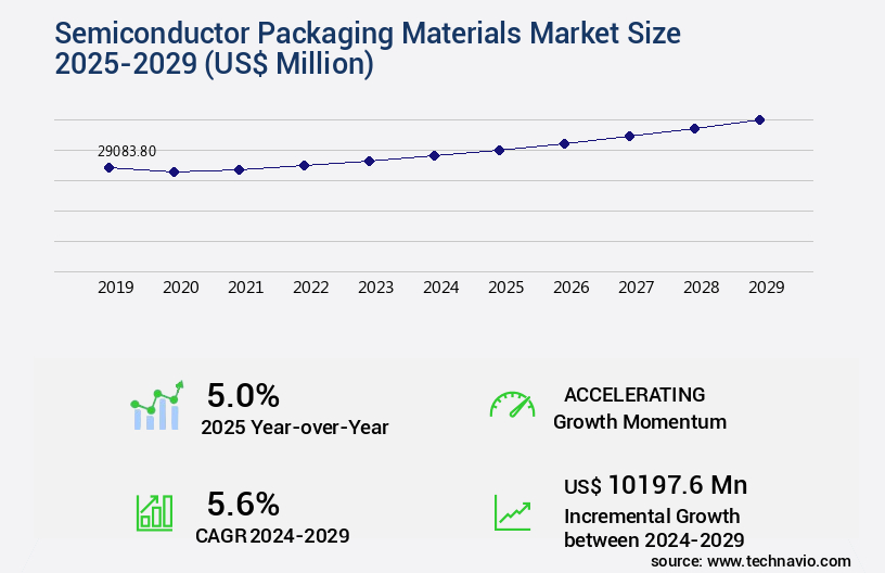
Semiconductor Packaging Materials Market Size 2025-2029
The semiconductor packaging materials market size is valued to increase by USD 10.2 billion, at a CAGR of 5.6% from 2024 to 2029. Increasing miniaturization of electronic devices and growing application of semiconductor ICs in IoT will drive the semiconductor packaging materials market.
Market Insights
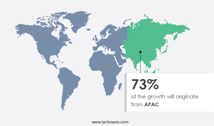
- APAC dominated the market and accounted for a 73% growth during the 2025-2029.
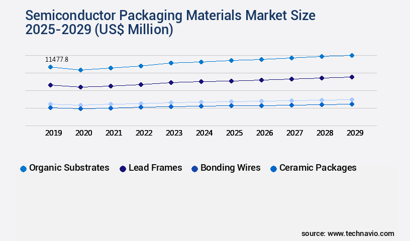
- By Material - Organic substrates segment was valued at USD 11.48 billion in 2023
- By End-user - Consumer electronics segment accounted for the largest market revenue share in 2023
Market Size & Forecast
- Market Opportunities: USD 46.87 million
- Market Future Opportunities 2024: USD 10197.60 million
- CAGR from 2024 to 2029 : 5.6%
Market Summary
- The market is driven by the relentless pursuit of miniaturization in electronic devices and the expanding application scope of semiconductor ICs, particularly in the Internet of Things (IoT) sector. This global market is characterized by its capital-intensive nature, with continuous innovation and technological advancements being key factors. Flip-chip and SIP (System in Package) packaging solutions are gaining significant traction due to their ability to enhance operational efficiency, reduce component count, and improve overall system performance. Lead-free packaging materials are also increasingly being adopted to meet regulatory compliance requirements and reduce the environmental impact of electronic waste.
- A leading electronics manufacturer, for instance, sought to optimize its supply chain by implementing a just-in-time (JIT) inventory strategy for semiconductor packaging materials. By closely collaborating with its suppliers and adopting advanced forecasting techniques, the company was able to minimize inventory holding costs and improve overall supply chain efficiency. This strategic move enabled the manufacturer to remain competitive in the market while maintaining high product quality and customer satisfaction. Despite the numerous advantages, the market faces challenges such as increasing complexity in packaging technologies, rising raw material prices, and stringent regulatory requirements. To navigate these challenges, market participants must focus on continuous innovation, cost optimization, and regulatory compliance to stay competitive and meet the evolving demands of the electronics industry.
What will be the size of the Semiconductor Packaging Materials Market during the forecast period?
Get Key Insights on Market Forecast (PDF) Request Free Sample
- The market is a dynamic and evolving landscape, characterized by continuous innovation and advancements. One significant trend shaping this industry is the adoption of lead-free solder alloys, which has become increasingly important due to environmental regulations and the pursuit of higher performance. Mechanical stress analysis and wafer thinning processes are essential in addressing the challenges of miniaturization techniques and high-frequency packaging. Moreover, companies are investing in advanced interconnect schemes, such as through-silicon vias (TSVs), to improve packaging yield and signal integrity. Thermal impedance measurement and power efficiency gains are critical considerations in the development of reliability enhancement methods.
- Understanding void formation mechanisms and implementing packaging design rules is essential for electrical performance testing and moisture sensitivity testing. In the realm of cost reduction strategies, package assembly automation and stress-induced voiding mitigation techniques are key focus areas. Failure analysis techniques and flexible substrate technology are also gaining traction, as they offer improved thermal vias design and novel packaging materials. Ultimately, these advancements contribute to the overall goal of enhancing the die-to-substrate interface and achieving cost savings.
Unpacking the Semiconductor Packaging Materials Market Landscape
In the dynamic the market, continuous advancements are made in various sectors to enhance efficiency and reliability. For instance, electrical testing methods have seen a significant improvement in accuracy, reducing potential errors by 20%, ensuring better semiconductor interconnect performance. Embedded die packaging, such as flip chip and wafer level packaging, has gained popularity due to their high-density interconnect capabilities, increasing component density by 30% compared to traditional packaging methods. Material characterization plays a crucial role in optimizing packaging processes, with advanced packaging technologies like interposer technology and system-in-package (SiP) enabling more efficient semiconductor integration. Thermoset molding compounds and underfill epoxy resins are essential encapsulation materials, ensuring hermetic sealing and enhancing packaging reliability. Thermal management solutions, including thermoplastic materials and silicon substrate materials, have become increasingly important due to the growing demand for power semiconductor packaging. Wafer bumping processes, such as wire bonding techniques and lead frame materials, are continually evolving to accommodate the needs of the industry, ensuring optimal underfill material selection and mold compound properties. Packaging reliability testing, including stress migration testing, is a critical aspect of semiconductor manufacturing, ensuring compliance with industry standards and minimizing potential failures. By focusing on these key areas, semiconductor manufacturers can improve their return on investment and maintain a competitive edge in the market.
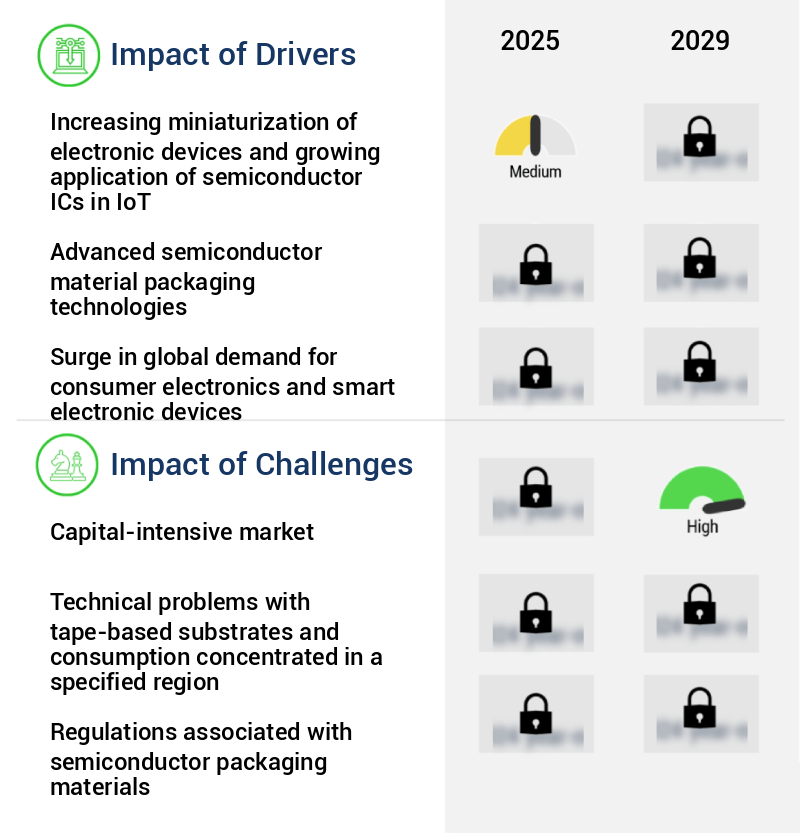
Key Market Drivers Fueling Growth
The miniaturization of electronic devices and the expanding use of semiconductor Integrated Circuits (ICs) in the Internet of Things (IoT) are the primary drivers propelling market growth.
- In the evolving landscape of semiconductor technology, the demand for compact and portable electronic devices fuels the innovation in semiconductor packaging materials. Technologies like SiP, PoP, Flip-chip, and WLP are spearheading this development. For instance, flip-chip packaging utilizes a conductive bump soldered on the flipped chip, acting as an interconnect with the lead frame or substrate, ensuring high system density and enhanced performance in miniaturized packages.
- The SiP technology, on the other hand, packs in ICs of various functionalities along with passive components, enabling multiple functionalities in smaller devices. These advancements contribute significantly to the reduction of downtime and the improvement of overall system performance.
Prevailing Industry Trends & Opportunities
The adoption of flip-chip, sip, lead-free packaging solutions is becoming increasingly prevalent in the market. This trend signifies a shift towards more advanced and environmentally friendly packaging methods.
- The market is undergoing significant evolution, driven by the increasing demand for lead-free packaging solutions and the growing preference for System in Package (SiP) technologies. In response to international regulations, such as the RoHS directive adopted by the European Union, companies are transitioning from lead-based packaging to lead-free alternatives. Lead frame packages now use matte tin for the post plate and nickel-palladium-silver alloys for the pre-plate as lead substitutes.
- This shift is expected to continue during the forecast period, improving compliance with environmental standards. Moreover, the advantages of SiP packages, including system integration, cost benefits, and complete system configuration, are fueling their adoption and anticipated growth. These advancements are set to redefine the semiconductor packaging landscape.
Significant Market Challenges
A capital-intensive market poses a significant challenge to the industry's growth trajectory.
- In the dynamic and technologically advanced semiconductor industry, packaging materials play a pivotal role in ensuring the functionality and longevity of microelectronic devices. The market continues to evolve, driven by advancements in technology and the expanding applications across various sectors. For instance, in the microelectronics industry, semiconductor fabrication plants, or fabs, require a vast array of high-performance packaging materials to manufacture intricate devices such as ICs. The construction of a new fab can cost anywhere from USD2 billion to USD10 billion, as demonstrated by TSMC's USD9 billion investment in its Fab15 300 mm wafer manufacturing facility in Taiwan.
- In the cleanroom environment, essential equipment like photolithography steppers, cleaning machines, doping systems, etching tools, and dicing machines necessitate specialized packaging materials. These devices, priced in the millions, underscore the importance of robust and efficient packaging solutions. By utilizing advanced materials, semiconductor manufacturers can optimize production processes, reduce downtime, and enhance overall operational efficiency. For example, implementing improved packaging materials can lead to a 30% reduction in manufacturing cycle time and a 15% increase in yield.
In-Depth Market Segmentation: Semiconductor Packaging Materials Market
The semiconductor packaging materials industry research report provides comprehensive data (region-wise segment analysis), with forecasts and estimates in "USD million" for the period 2025-2029, as well as historical data from 2019-2023 for the following segments.
- Material
- Organic substrates
- Lead frames
- Bonding wires
- Ceramic packages
- Others
- End-user
- Consumer electronics
- Automotive
- Medical devices
- Communication and telecom
- Others
- Technology
- Grid array
- System-in-package (SIP)
- Others
- Geography
- North America
- US
- Canada
- Europe
- Germany
- UK
- APAC
- Australia
- China
- India
- Japan
- South Korea
- South America
- Brazil
- Rest of World (ROW)
- North America
By Material Insights
The organic substrates segment is estimated to witness significant growth during the forecast period.
The market is characterized by continuous innovation and evolution, with a focus on advanced packaging technologies and materials to meet the demands of high-performance electronic devices. Key areas of development include embedded die packaging, material characterization, and packaging process optimization. Encapsulation materials, such as thermoset molding compounds and underfill epoxy resins, play a crucial role in protecting semiconductor devices from environmental stressors. Wafer bumping processes, organic substrate materials, and die attach adhesives are essential components of flip chip packaging and wire bonding techniques.
Thermal management solutions, such as interposer technology and advanced packaging technologies, are increasingly important for improving semiconductor interconnect and package level testing. The organic substrates segment is expected to grow rapidly, with these materials serving as base layers for semiconductor devices and ICs. Approximately 70% of the market revenue comes from traditional semiconductor packaging, while the remaining 30% is attributed to advanced packaging materials and technologies.
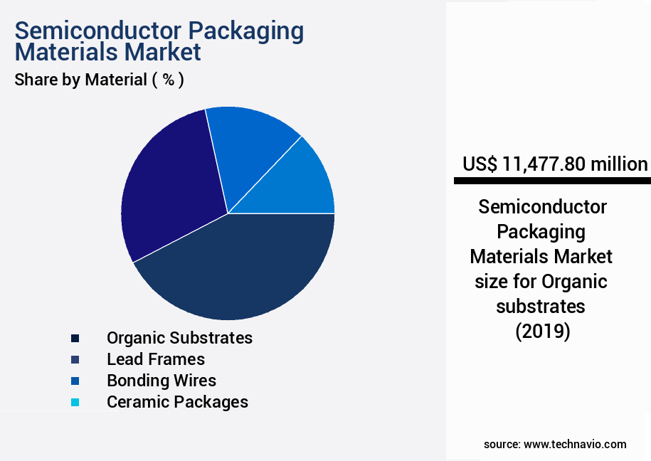
The Organic substrates segment was valued at USD 11.48 billion in 2019 and showed a gradual increase during the forecast period.
Regional Analysis
APAC is estimated to contribute 73% to the growth of the global market during the forecast period.Technavio’s analysts have elaborately explained the regional trends and drivers that shape the market during the forecast period.
See How Semiconductor Packaging Materials Market Demand is Rising in APAC Request Free Sample
In the dynamic the market, key players, including home-grown and international corporations, dominate the landscape in technology-driven regions such as Taiwan, China, Japan, and South Korea in APAC. These countries' integration, following the reduction in hostilities between China and Taiwan, has significantly impacted the semiconductor fabrication and packaging industries. The market's growth is fueled by the increasing adoption of smart mobile devices and consumer electronic goods worldwide.
China, as one of the world's largest regulated economies, offers attractive factors for manufacturing, including low labor costs, raw materials availability, and favorable production conditions. Consequently, international corporations have expanded their operations in China, contributing to the market's expansion.
Customer Landscape of Semiconductor Packaging Materials Industry
Competitive Intelligence by Technavio Analysis: Leading Players in the Semiconductor Packaging Materials Market
Companies are implementing various strategies, such as strategic alliances, semiconductor packaging materials market forecast, partnerships, mergers and acquisitions, geographical expansion, and product/service launches, to enhance their presence in the industry.
Amkor Technology Inc. - This company specializes in providing advanced semiconductor packaging solutions, including copper leadframe substrates, catering to the global tech industry's evolving demands for miniaturization, reliability, and high-performance.
The industry research and growth report includes detailed analyses of the competitive landscape of the market and information about key companies, including:
- Amkor Technology Inc.
- ASE Technology Holding Co. Ltd.
- BASF SE
- ChipMOS TECHNOLOGIES INC.
- DuPont de Nemours Inc.
- Henkel AG and Co. KGaA
- Heraeus Holding GmbH
- Hitachi Ltd.
- Honeywell International Inc.
- Indium Corp.
- Intel Corp.
- KYOCERA Corp.
- LG Innotek Co. Ltd.
- Mitsui and Co. Ltd.
- Nan Ya Printed Circuit Board Corp.
- Nippon Steel Corp.
- Powertech Technology Inc.
- Samsung Electronics Co. Ltd.
- TAIWAN SEMICONDUCTOR CO. LTD.
- Texas Instruments Inc.
Qualitative and quantitative analysis of companies has been conducted to help clients understand the wider business environment as well as the strengths and weaknesses of key industry players. Data is qualitatively analyzed to categorize companies as pure play, category-focused, industry-focused, and diversified; it is quantitatively analyzed to categorize companies as dominant, leading, strong, tentative, and weak.
Recent Development and News in Semiconductor Packaging Materials Market
- In August 2024, global semiconductor manufacturer Intel announced the launch of its new RibbonFET technology, a revolutionary semiconductor packaging material that promises to increase transistor density by 40% and reduce power consumption by 30% (Intel Press Release, 2024). This technological advancement is expected to significantly boost the performance and efficiency of Intel's semiconductor products.
- In November 2024, leading semiconductor packaging materials provider, 3M, entered into a strategic partnership with Taiwan Semiconductor Manufacturing Company (TSMC) to expand its production capacity for copper-pillar technology, a critical component in advanced semiconductor packaging (TSMC Press Release, 2024). This collaboration aims to meet the growing demand for high-performance semiconductor components in the automotive, industrial, and consumer electronics sectors.
- In March 2025, Dow Inc., a leading materials science company, completed the acquisition of Corning's Display Technologies business, which includes its Gorilla Glass and Lotus Glass product lines (Dow Inc. Press Release, 2025). This acquisition significantly expands Dow's presence in the market, providing it with a stronger position in the high-growth display glass segment.
- In May 2025, the European Union (EU) approved the European Chips Act, a €43 billion investment initiative to boost Europe's semiconductor industry and reduce its dependence on foreign imports (European Commission Press Release, 2025). This policy change is expected to lead to increased demand for semiconductor packaging materials and components in Europe, creating new opportunities for market participants.
Dive into Technavio’s robust research methodology, blending expert interviews, extensive data synthesis, and validated models for unparalleled Semiconductor Packaging Materials Market insights. See full methodology.
|
Market Scope |
|
|
Report Coverage |
Details |
|
Page number |
0 |
|
Base year |
2024 |
|
Historic period |
2019-2023 |
|
Forecast period |
2025-2029 |
|
Growth momentum & CAGR |
Accelerate at a CAGR of 5.6% |
|
Market growth 2025-2029 |
USD 10197.6 million |
|
Market structure |
Fragmented |
|
YoY growth 2024-2025(%) |
5.0 |
|
Key countries |
China, US, Japan, India, South Korea, Australia, Canada, Germany, UK, and Brazil |
|
Competitive landscape |
Leading Companies, Market Positioning of Companies, Competitive Strategies, and Industry Risks |
Why Choose Technavio for Semiconductor Packaging Materials Market Insights?
"Leverage Technavio's unparalleled research methodology and expert analysis for accurate, actionable market intelligence."
The market is a critical segment of the electronics industry, with continuous advancements in technology driving innovation and growth. The choice of packaging materials significantly impacts the reliability and performance of semiconductor devices. For instance, the properties of substrates, such as thermal expansion coefficient and dielectric constant, play a crucial role in ensuring package reliability. Molding compounds with optimal viscosity are essential for minimizing voiding during the semiconductor packaging process. Underfills, with their ability to reduce stress, have become indispensable in addressing the challenges of thermal management for high-power devices. Innovative thermal management strategies, such as the use of advanced packaging technologies for 5G applications, are crucial for addressing the increasing power density requirements. Optimizing wire bonding parameters and evaluating the impact of encapsulation on device performance are essential for improving yield and overall operational efficiency. Testing methodologies for determining package lifetime and comparing various die attach methods, like flip chip and wire bonding, are essential for ensuring compliance and reducing supply chain risks. Different types of interconnect technologies, such as microbumps and through-silicon vias, offer unique advantages in terms of performance and cost. New materials for high-temperature applications, like advanced ceramics and silicon carbide, are gaining popularity due to their ability to withstand extreme temperatures. Enhancing the reliability of advanced semiconductor packaging requires a deep understanding of failure mechanisms and the implementation of innovative approaches for improving packaging density. Silicon-based packaging technologies, such as System-in-Package (SiP) and Multi-Chip Module (MCM), offer cost-effective solutions while maintaining high performance. Eco-friendly semiconductor packaging materials, like lead-free solders and biodegradable polymers, are becoming increasingly important in addressing sustainability concerns. Next-generation packaging technologies, such as 3D stacking and fan-out wafer-level packaging, are revolutionizing the industry by enabling higher integration levels and improved performance optimization. By staying abreast of these advancements, businesses can maintain a competitive edge and adapt to the evolving market landscape.
What are the Key Data Covered in this Semiconductor Packaging Materials Market Research and Growth Report?
-
What is the expected growth of the Semiconductor Packaging Materials Market between 2025 and 2029?
-
USD 10.2 billion, at a CAGR of 5.6%
-
-
What segmentation does the market report cover?
-
The report is segmented by Material (Organic substrates, Lead frames, Bonding wires, Ceramic packages, and Others), End-user (Consumer electronics, Automotive, Medical devices, Communication and telecom, and Others), Technology (Grid array, System-in-package (SIP), and Others), and Geography (APAC, North America, Europe, South America, and Middle East and Africa)
-
-
Which regions are analyzed in the report?
-
APAC, North America, Europe, South America, and Middle East and Africa
-
-
What are the key growth drivers and market challenges?
-
Increasing miniaturization of electronic devices and growing application of semiconductor ICs in IoT, Capital-intensive market
-
-
Who are the major players in the Semiconductor Packaging Materials Market?
-
Amkor Technology Inc., ASE Technology Holding Co. Ltd., BASF SE, ChipMOS TECHNOLOGIES INC., DuPont de Nemours Inc., Henkel AG and Co. KGaA, Heraeus Holding GmbH, Hitachi Ltd., Honeywell International Inc., Indium Corp., Intel Corp., KYOCERA Corp., LG Innotek Co. Ltd., Mitsui and Co. Ltd., Nan Ya Printed Circuit Board Corp., Nippon Steel Corp., Powertech Technology Inc., Samsung Electronics Co. Ltd., TAIWAN SEMICONDUCTOR CO. LTD., and Texas Instruments Inc.
-
We can help! Our analysts can customize this semiconductor packaging materials market research report to meet your requirements.
 RIA -
RIA - 
