
Photoresist Market Size 2024-2028
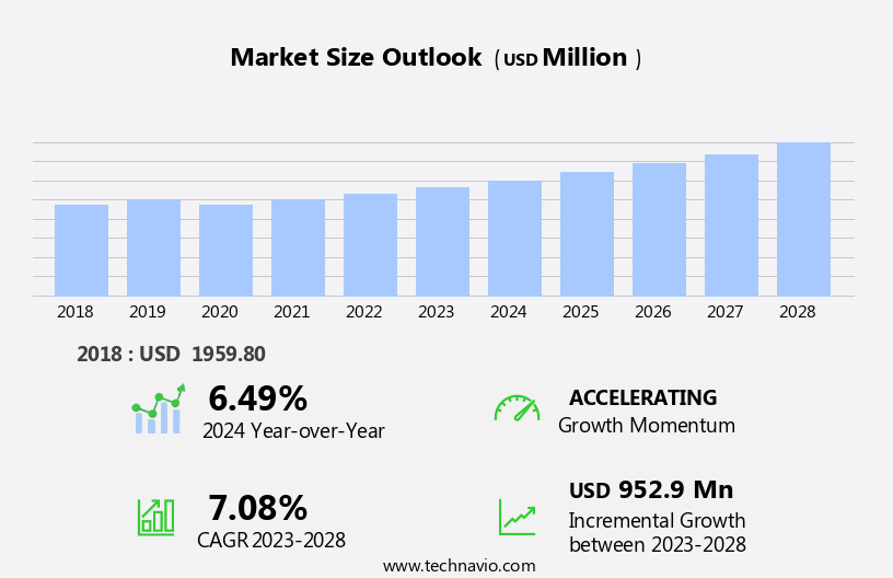
The photoresist market size is forecast to increase by USD 952.9 million, at a CAGR of 7.08% between 2023 and 2028.
- The market is driven by the burgeoning demand for electronics, particularly in the consumer electronics and IT industries. This increasing need for advanced technology devices fuels the market's growth, as photoresist plays a crucial role in the production of semiconductors and printed circuit boards. However, the market faces challenges due to the slowdown in the semiconductor industry growth. This trend is attributed to the maturing market and economic uncertainties, which may impact the demand for new technology devices. Moreover, advancements in material technology pose challenges to traditional photoresist suppliers, necessitating continuous innovation and adaptation to maintain market competitiveness.
- Companies in the market must navigate these challenges by focusing on research and development, cost optimization, and strategic partnerships to capitalize on emerging opportunities and maintain a strong market position.
What will be the Size of the Photoresist Market during the forecast period?
Explore in-depth regional segment analysis with market size data - historical 2018-2022 and forecasts 2024-2028 - in the full report.
Request Free Sample
The market continues to evolve, driven by the constant advancements in technology and the expanding applications across various sectors. Spectroscopic techniques and chemical analysis play a crucial role in material characterization, ensuring the optimal performance of underlayer coatings and plasma etching processes in semiconductor manufacturing. Throughput optimization is a key focus, with the integration of adhesion promoters and resolution enhancement techniques to improve photoresist materials' properties in optical lithography. Nanoimprint lithography and other advanced lithographic techniques, such as electron beam lithography and directed self-assembly, are revolutionizing the industry. Process control is paramount, with development processes meticulously managed to minimize line edge roughness and maintain critical dimension (CD) accuracy.
Post-exposure bake (PEB) and wafer processing are essential steps in the etching processes, with anti-reflective coatings (ARC) and process monitoring ensuring efficient and effective manufacturing. Safety protocols are stringently enforced in cleanroom environments, with resist stripping and defect inspection crucial for maintaining high yield and quality control. Negative and positive photoresists, each with their unique advantages, are employed to cater to diverse manufacturing requirements. Cost reduction strategies, such as waste management and the adoption of dry etching and ion beam lithography, are ongoing priorities for market participants. Environmental regulations continue to shape the industry, with ongoing research and innovation in photoresist sensitivity, topcoat layers, and environmental-friendly alternatives.The market's continuous dynamism is further highlighted by the integration of advanced technologies, such as immersion lithography, to push the boundaries of what is possible in semiconductor manufacturing.
How is this Photoresist Industry segmented?
The photoresist industry research report provides comprehensive data (region-wise segment analysis), with forecasts and estimates in "USD million" for the period 2024-2028, as well as historical data from 2018-2022 for the following segments.
- Type
- ArF photoresist
- KrF photoresist
- G-line and I-line photoresist
- EUV photoresist
- Application
- Semiconductors
- Liquid Crystal Displays (LCDs)
- Printed Circuit Boards (PCBs)
- Others
- End-user Industry
- Electricals and Electronics
- Automobiles
- Packaging
- Others
- Geography
- North America
- US
- Canada
- Mexico
- Europe
- France
- Germany
- Italy
- UK
- APAC
- China
- Japan
- South Korea
- Rest of World (ROW)
- North America
By Type Insights
The arf photoresist segment is estimated to witness significant growth during the forecast period.
In the realm of semiconductor manufacturing, ArF immersion lithography plays a pivotal role in scaling electronic components by utilizing a fluid layer between the wafer and optics to enhance resolution. The miniaturization of ICs is the primary driving force behind this market segment, as major foundries prioritize delivering smaller node-sized ICs. The shrinking size of these components poses a challenge for developers due to increased design complexity. Lithography facilitates the significant reduction of IC geometries through multi-patterning, enabling the production of 10nm process node-sized ICs. Spectroscopic techniques and chemical analysis are employed to ensure process control during lithography, while underlayer coatings and plasma etching optimize throughput and enhance resolution.
Adhesion promoters and topcoat layers are crucial for maintaining the integrity of the photoresist material during various development processes. Material characterization and resist thickness measurement are essential for maintaining critical dimensions and improving yield. Safety protocols and cleanroom environments are integral to the process, with resist stripping and defect inspection ensuring the highest quality standards. Environmental regulations mandate the implementation of waste management strategies and cost reduction techniques, such as dry etching and ion beam lithography, to minimize the environmental footprint. Photoresist sensitivity and line edge roughness are critical factors in optimizing the lithography process, with post-exposure bake and photomask manufacturing playing essential roles in achieving the desired results.Process monitoring and anti-reflective coatings are integral to maintaining process consistency and enhancing overall efficiency.
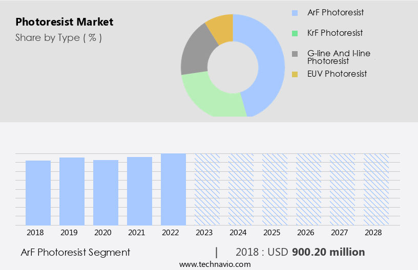
The ArF photoresist segment was valued at USD 900.20 million in 2018 and showed a gradual increase during the forecast period.
Regional Analysis
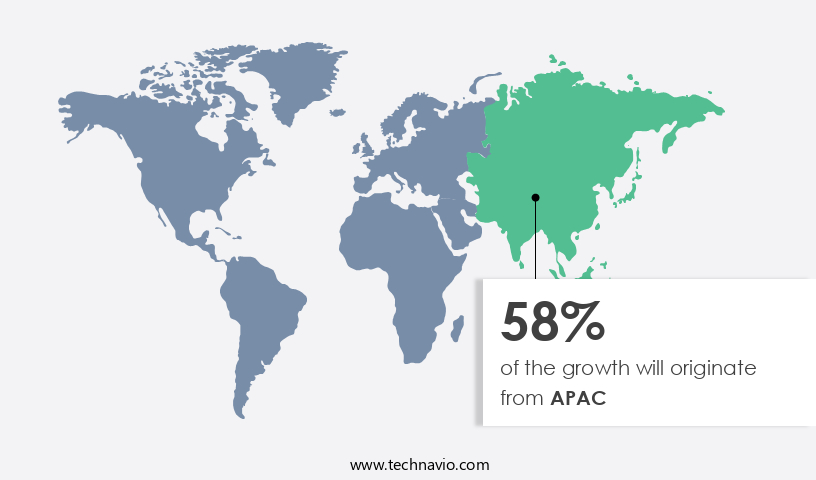
APAC is estimated to contribute 58% to the growth of the global market during the forecast period.Technavio's analysts have elaborately explained the regional trends and drivers that shape the market during the forecast period.
In the dynamic semiconductor manufacturing landscape of 2023, the market experiences significant growth. This expansion is driven by the increasing demand for integrated chips (ICs) and printed circuit boards (PCBs) in the semiconductor industry, particularly in the Asia Pacific region. Photoresist materials are essential in this process, enabling precise patterning and etching of circuit designs. The semiconductor industry's growth is fueled by the surge in demand for ICs from fabless foundries, spurred by the expansion of Chinese smartphone manufacturers like Huawei, Lenovo, OnePlus, and OPPO. These firms offer high-quality, competitively priced smartphones, challenging market leaders Apple and SAMSNG.
Underlayer coatings and plasma etching are crucial techniques in this process, ensuring accurate and efficient etching of photoresist layers. Throughput optimization, adhesion promoters, and resolution enhancement techniques further enhance the manufacturing process. Material characterization and process control are essential for maintaining critical dimensions (CD) and improving yield. Process monitoring, photomask manufacturing, and safety protocols ensure the production of high-quality, defect-free wafers. Wafer processing involves various etching processes, including wet etching and dry etching, as well as the application of anti-reflective coatings (arc). Environmental regulations necessitate the use of immersion lithography and other advanced techniques, such as electron beam lithography and nanoimprint lithography, to minimize waste and improve cost reduction strategies.
Photoresist sensitivity and topcoat layers are critical factors in achieving optimal results. In this evolving market, process innovation and quality control remain key priorities. Negative and positive photoresists, chemically amplified resist, and development processes are continually refined to meet the demands of the industry. The integration of advanced techniques, such as directed self-assembly and ion beam lithography, further enhances the capabilities of photoresist materials.
Market Dynamics
Our researchers analyzed the data with 2023 as the base year, along with the key drivers, trends, and challenges. A holistic analysis of drivers will help companies refine their marketing strategies to gain a competitive advantage.
The global photoresist market size and forecast projects growth, driven by photoresist market trends 2024-2028. B2B photoresist supply solutions leverage advanced photoresist technologies for precision. Photoresist market growth opportunities 2025 include photoresists for semiconductor manufacturing and photoresists for electronics, meeting demand. Photoresist supply chain software optimizes operations, while photoresist market competitive analysis highlights key manufacturers. Sustainable photoresist practices align with eco-friendly chemical trends. Photoresist regulations 2024-2028 shapes photoresist demand in Asia 2025. High-performance photoresist solutions and premium photoresist insights boost adoption. Photoresists for displays and customized photoresist formulations target niches. Photoresist market challenges and solutions address quality, with direct procurement strategies for photoresists and photoresist pricing optimization enhancing profitability. Data-driven photoresist market analytics and advanced photoresist technology trends drive innovation.
What are the key market drivers leading to the rise in the adoption of Photoresist Industry?
- The increasing demand for electronics serves as the primary catalyst for market growth.
- The market is experiencing significant growth due to the increasing demand for advanced electronics in various industries. The latest technology innovations, such as 3D printing, drones, and conductive polymers, necessitate faster, smaller, and more cost-effective manufacturing processes. In response, companies are enhancing the quality and performance of photoresist materials through advancements in technology and equipment. Negative photoresist, a key type of photoresist, is widely used in the production of semiconductors and flat panel displays. Topcoat layers are applied to improve the sensitivity and durability of the photoresist, ensuring precise and consistent etching processes, including dry etching and ion beam lithography.
- Environmental regulations continue to play a crucial role in the market, with a focus on waste management and cost reduction strategies. Immersive lithography, which uses water or other solvents to develop the photoresist, is gaining popularity due to its ability to produce smaller and more intricate patterns. companies are investing in research and development to meet the evolving demands of the market and maintain a competitive edge. Quality control is a top priority in the market, with companies implementing rigorous testing and inspection processes to ensure the highest standards of product consistency and reliability. The market is expected to continue growing as the demand for advanced electronics increases and technology continues to evolve.
What are the market trends shaping the Photoresist Industry?
- Advancements in material technology are currently shaping market trends. The continuous evolution of materials is a significant factor driving innovation and growth in various industries.
- Direct incident beam lithography, a new technology, utilizes the "direct-wire" method to create intricate three-dimensional (3D) lithographic patterns of various nanoparticle materials, such as metals, semiconductors, insulators, and magnetic materials. This technology offers numerous advantages, including its quick and easy patterning process, the versatility of writing modes, the wide range of applications, and the flexibility and utility in nano/microfabrication. Applications include magnetics, photonics/plasmonics, 3D electronic structures, and MEMS/NEMS. Advancements in material technology have significantly impacted semiconductor manufacturing and the production of electrical devices. The shift from MEMS to bio-NEMS/MEMS has driven the innovation of cutting-edge materials for patterning using photoresist and photoresist ancillaries.
- Spectroscopic techniques and chemical analysis are essential in the development and optimization of underlayer coatings, plasma etching, and wet etching processes. Resolution enhancement techniques and adhesion promoters play crucial roles in ensuring successful patterning. Direct incident beam lithography's immersive and harmonious approach to fabrication makes it a valuable tool in the ongoing advancements of nano/microelectronics.
What challenges does the Photoresist Industry face during its growth?
- The semiconductor industry's growth is being significantly challenged by a deceleration in its own expansion rate.
- The market is experiencing significant shifts due to various factors influencing the semiconductor and automotive industries. The decline in demand for consumer electronics and automobiles, coupled with a shortage of skilled workforce, has negatively impacted the profitability of manufacturing companies and, consequently, the demand for photoresist materials. These dynamics can have a profound effect on the manufacturing process and investments in capital goods. Moreover, external factors such as the ongoing trade war between China and the US and the global impact of COVID-19 are anticipated to influence the output of the semiconductor industry worldwide. In the context of photoresist, this could lead to disruptions in the supply chain and potential price fluctuations.
- Process control is a critical aspect of photoresist application, with factors such as resist thickness, line edge roughness, post-exposure bake (PEB), and wafer processing playing significant roles. Advanced technologies like directed self-assembly and electron beam lithography are also gaining traction to improve process control and efficiency. Manufacturers are continually seeking innovative solutions to address the challenges posed by these market dynamics while maintaining high-quality standards. Effective process control, development processes, and etching processes are essential to mitigate the risks and ensure the long-term sustainability of the market.
Exclusive Customer Landscape
The photoresist market forecasting report includes the adoption lifecycle of the market, covering from the innovator's stage to the laggard's stage. It focuses on adoption rates in different regions based on penetration. Furthermore, the photoresist market report also includes key purchase criteria and drivers of price sensitivity to help companies evaluate and develop their market growth analysis strategies.

Customer Landscape
Key Companies & Market Insights
Companies are implementing various strategies, such as strategic alliances, photoresist market forecast, partnerships, mergers and acquisitions, geographical expansion, and product/service launches, to enhance their presence in the industry.
AGC Inc. - This company specializes in providing advanced photoresists, including SPR 3, SPR 700, and MCPR, to the semiconductor industry. These photoresists enable precise pattern definition during photolithography processes, enhancing manufacturing efficiency and product quality. The company's offerings cater to various applications, ensuring technological innovation and process optimization for clients.
The industry research and growth report includes detailed analyses of the competitive landscape of the market and information about key companies, including:
- AGC Inc.
- Allresist GmbH
- Applied Materials Inc.
- DJ MicroLaminates Inc.
- DuPont de Nemours Inc.
- Everlight Chemical Industrial Co
- FUJIFILM Corp.
- JSR Corp.
- KLA Corp.
- Lam Research Corp.
- LG Chem Ltd.
- Merck KGaA
- Micro resist technology GmbH
- Mitsui Chemicals Inc.
- PhiChem Corp.
- Shenzhen RongDa Photosensitive Science and Technology Co. Ltd.
- Shin Etsu Chemical Co. Ltd.
- Sumitomo Chemical Co. Ltd.
- Suzhou Crystal Clear Chemical Co. Ltd
- TOKYO OHKA KOGYO CO. LTD.
Qualitative and quantitative analysis of companies has been conducted to help clients understand the wider business environment as well as the strengths and weaknesses of key industry players. Data is qualitatively analyzed to categorize companies as pure play, category-focused, industry-focused, and diversified; it is quantitatively analyzed to categorize companies as dominant, leading, strong, tentative, and weak.
Recent Development and News in Photoresist Market
- In January 2024, Merck KGaA, a leading supplier of photoresists, announced the launch of its new generation of SU-8 photoresists, named SU-8 3050, which offers enhanced resolution and sensitivity, addressing the increasing demand for miniaturization in semiconductor manufacturing (Merck KGaA press release).
- In March 2024, Intel Corporation and Tokyo Electron Limited, major players in the semiconductor industry, formed a strategic collaboration to develop advanced photoresist technologies, aiming to improve the performance and reduce the cost of their manufacturing processes (Intel press release).
- In May 2024, LG Chem, a South Korean chemical company, completed the acquisition of a 49% stake in Hankook M&S, a leading photoresist manufacturer in South Korea, expanding its presence in the market and strengthening its position in the semiconductor industry (Yonhap News Agency).
- In February 2025, the European Union approved the renewal of the Registration, Evaluation, Authorization and Restriction of Chemicals (REACH) registration for microelectronics photoresists, ensuring the continued availability and use of these essential materials in the European market (European Chemicals Agency press release).
Research Analyst Overview
- The market experiences dynamic activity driven by advancements in laser sources, high-NA optics, and next-generation lithography. Defect density remains a critical concern, with continuous efforts to improve resist profile and overlay accuracy through soft bake, substrate preparation, and advanced patterning techniques. Novolac resin and PMMA are key resist materials, with spin coating and exposure systems playing essential roles in high-throughput manufacturing. Laser sources and high-NA optics enable better linewidth control and pattern fidelity. Diazonaphthoquinone (DNQ) and other photoinitiators facilitate self-aligned patterning, enhancing manufacturing efficiency.
- AI and modeling & simulation are increasingly utilized for process optimization and defect prediction. 3D printing and advanced resist materials like PMMA expand the market's scope. Linewidth control and pattern fidelity are crucial for producing high-performance semiconductors and advanced electronics. The integration of AI, self-aligned patterning, and high-throughput manufacturing ensures continued innovation and growth in the photoresist industry.
Dive into Technavio's robust research methodology, blending expert interviews, extensive data synthesis, and validated models for unparalleled Photoresist Market insights. See full methodology.
|
Market Scope |
|
|
Report Coverage |
Details |
|
Page number |
157 |
|
Base year |
2023 |
|
Historic period |
2018-2022 |
|
Forecast period |
2024-2028 |
|
Growth momentum & CAGR |
Accelerate at a CAGR of 7.08% |
|
Market growth 2024-2028 |
USD 952.9 million |
|
Market structure |
Concentrated |
|
YoY growth 2023-2024(%) |
6.49 |
|
Key countries |
China, US, Japan, South Korea, Germany, Canada, Mexico, UK, France, and Italy |
|
Competitive landscape |
Leading Companies, Market Positioning of Companies, Competitive Strategies, and Industry Risks |
What are the Key Data Covered in this Photoresist Market Research and Growth Report?
- CAGR of the Photoresist industry during the forecast period
- Detailed information on factors that will drive the growth and forecasting between 2024 and 2028
- Precise estimation of the size of the market and its contribution of the industry in focus to the parent market
- Accurate predictions about upcoming growth and trends and changes in consumer behaviour
- Growth of the market across APAC, North America, Europe, South America, and Middle East and Africa
- Thorough analysis of the market's competitive landscape and detailed information about companies
- Comprehensive analysis of factors that will challenge the photoresist market growth of industry companies
We can help! Our analysts can customize this photoresist market research report to meet your requirements.
 RIA -
RIA - 
