Nanoimprint Lithography (NIL) System Market Size 2024-2028
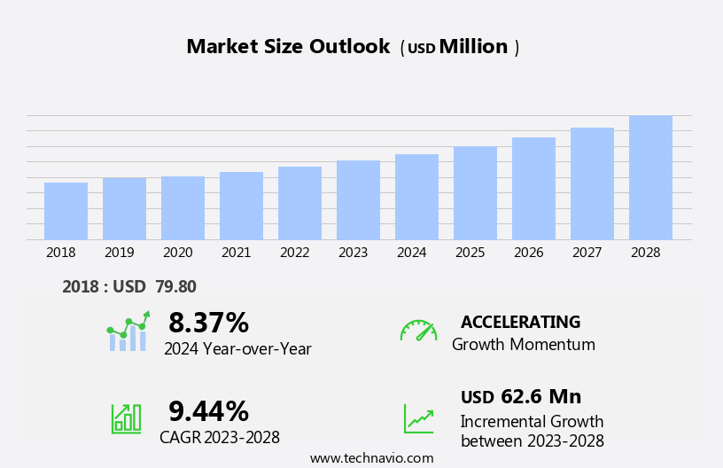
The nanoimprint lithography (NIL) system market size is forecast to increase by USD 62.6 million, at a CAGR of 9.44% between 2023 and 2028.
- The market is experiencing significant growth due to the emergence of miniaturized semiconductor components and the increasing adoption of Internet of Things (IoT) technology. NIL systems offer advantages such as high resolution, large area printing, and the ability to print on various substrates, making them an attractive solution for manufacturing these advanced components. The IoT sector's expansion is also driving demand for NIL systems, as the technology enables the production of smaller, more efficient sensors and devices. However, the NIL System Market faces challenges, including the volatile nature of the semiconductor industry. Market fluctuations can impact investment decisions and the overall growth trajectory of the market.
- Additionally, the high cost of NIL equipment and the complex nature of the technology pose challenges for smaller players and new entrants. Despite these obstacles, opportunities exist for companies to capitalize on the market's growth by investing in research and development, collaborating with industry partners, and offering cost-effective solutions to address the challenges faced by the industry.
What will be the Size of the Nanoimprint Lithography (NIL) System Market during the forecast period?
Nanoimprint Lithography (NIL) is a continuously evolving technology that offers significant advancements in high-resolution patterning for various industries. The NIL system utilizes a master mold to transfer intricate patterns onto substrates, enabling the production of subwavelength features and high pattern densities. This technology has gained traction in sectors such as data storage, thermal NIL, biomedical devices, and organic electronics, among others. Nil development is ongoing, with a focus on optimizing process parameters to enhance yield and reduce defect density. High-volume manufacturing and cost-effective manufacturing are key areas of interest, as Nil equipment manufacturers strive to make this technology accessible to a wider range of industries.
The NIL industry is witnessing the emergence of new applications, including flexible electronics and roll-to-roll manufacturing. The technology roadmap for Nil includes the integration of advanced materials and process technologies, such as soft lithography and pattern transfer efficiency enhancements. Semiconductor manufacturing and display technology are also exploring the potential of NIL for high-resolution patterning. The future trends in Nil include the integration of advanced materials, the development of new tools, and the optimization of the Nil process to meet the evolving demands of various industries. Nil technology's continuous evolution is driven by the need for smaller feature sizes, higher pattern densities, and improved manufacturing efficiency. The ongoing research and development efforts in this field are expected to lead to new breakthroughs and applications, making Nil a dynamic and exciting area of study.
How is this Nanoimprint Lithography (NIL) System Industry segmented?
The nanoimprint lithography (NIL) system industry research report provides comprehensive data (region-wise segment analysis), with forecasts and estimates in "USD million" for the period 2024-2028, as well as historical data from 2018-2022 for the following segments.
- Application
- Optical equipment
- Consumer electronics
- Medical devices
- Wearable devices
- Others
- Type
- Hot embossing
- UV-based nanoimprint lithographys
- Micro contact printing
- Geography
- North America
- US
- Europe
- Germany
- UK
- APAC
- China
- Japan
- Rest of World (ROW)
- North America
By Application Insights
The optical equipment segment is estimated to witness significant growth during the forecast period.
Nanoimprint Lithography (NIL) systems have gained significant traction in various industries due to their ability to achieve high-resolution patterning and subwavelength features. In the field of data storage, NIL is being explored for the manufacturing of high-density magnetic recording media and optical data storage devices. Thermal NIL is particularly suitable for this application due to its ability to pattern large areas at high temperatures. Biomedical devices are another area where NIL is making an impact, with its potential to create complex microstructures for lab-on-a-chip applications and tissue engineering. Soft lithography, a type of NIL, is commonly used in this field due to its compatibility with biological materials.
The semiconductor manufacturing industry is also embracing NIL for the production of advanced components, such as high-performance microprocessors and memory devices. Wafer level NIL is a popular choice for this application due to its ability to pattern entire wafers at once, increasing productivity and reducing costs. NIL technology is also playing a crucial role in the development of organic electronics and flexible electronics. Organic materials require gentle processing conditions, which are well-suited to NIL. NIL tools can pattern organic materials with high pattern transfer efficiency, making them ideal for producing organic transistors, solar cells, and other organic electronic devices.
Display technology is another area where NIL is making a significant impact. NIL systems can pattern high-resolution patterns on large areas, making them suitable for producing high-definition displays. NIL research is also focusing on developing NIL systems for roll-to-roll manufacturing, which can produce flexible displays at a lower cost than traditional manufacturing methods. NIL process optimization is a key focus area for the industry, with researchers working to improve pattern transfer, reduce line edge roughness, and increase yield. Defect density is a critical factor in high-volume manufacturing, and NIL systems are being developed to minimize defects and improve overall manufacturing efficiency.
The future trends in NIL include its application in emerging areas such as printed electronics and emerging applications in the biomedical field. NIL systems are expected to become more cost-effective and accessible, making them a viable alternative to traditional lithography methods. Master molds, a critical component of NIL, are being developed using advanced materials and manufacturing techniques to improve pattern transfer and reduce costs. Overall, NIL is poised to play a significant role in the future of technology manufacturing, with applications ranging from data storage to display technology and beyond.
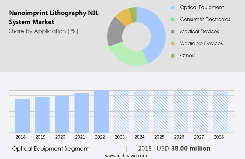
The Optical equipment segment was valued at USD 38.00 million in 2018 and showed a gradual increase during the forecast period.
Regional Analysis
Europe is estimated to contribute 42% to the growth of the global market during the forecast period. Technavio's analysts have elaborately explained the regional trends and drivers that shape the market during the forecast period.
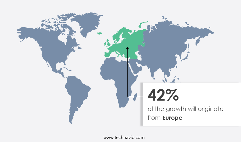
Nanoimprint lithography (NIL) systems have gained significant traction in various industries due to their ability to deliver high-resolution patterning and subwavelength features. In the European market, NIL systems hold a prominent position, particularly in Western Europe, which accounted for the largest market share in 2023. This dominance can be attributed to the region's robust semiconductor manufacturing sector, increasing investment in advanced technologies, and growing demand for smart devices. For instance, Intel's recent announcement to invest â¬70 billion (USD80 billion) in the European Union over the next decade is a testament to this trend. Moreover, the adoption of digital technologies such as artificial intelligence, augmented and virtual reality, and organic electronics is driving the growth of the NIL industry.
In the biomedical sector, NIL systems are being used to develop soft lithography for creating complex structures in medical devices. NIL technology's roadmap includes process optimization, wafer level NIL, roll-to-roll NIL, and high-volume manufacturing, making it a cost-effective alternative to traditional lithography methods like optical lithography. NIL research continues to focus on improving pattern transfer efficiency, feature size, and pattern density, leading to emerging applications in flexible electronics, printed electronics, and display technology. The future trends include the development of master molds and the integration of NIL systems with other advanced manufacturing technologies.
Market Dynamics
Our researchers analyzed the data with 2023 as the base year, along with the key drivers, trends, and challenges. A holistic analysis of drivers will help companies refine their marketing strategies to gain a competitive advantage.
What are the key market drivers leading to the rise in the adoption of Nanoimprint Lithography (NIL) System Industry?
- The miniaturization of semiconductor components serves as the primary catalyst for market growth. Nanoimprint Lithography (NIL) systems play a pivotal role in the semiconductor industry as the demand for miniaturized electronic components grows. With the focus on manufacturing smaller, more power-efficient personal electronics, semiconductor manufacturers are striving to reduce the size of devices without compromising performance. Integrated circuits (ICs) and chips, including LED displays, are essential components that need to be compact yet deliver superior performance. NIL, a versatile and cost-effective lithography technique, offers high-resolution patterning and high-density feature sizes, making it an ideal choice for producing advanced semiconductor components.
- The ongoing research in the NIL industry aims to optimize the process for mass production, ensuring consistent and high-quality results. The importance of NIL systems in the semiconductor industry is underscored by their ability to meet the increasing demand for miniaturized components without compromising performance or power consumption.
What are the market trends shaping the Nanoimprint Lithography (NIL) System Industry?
- The IoT market is experiencing significant growth in adoption, representing an emerging trend in technology. This expansion signifies a notable shift in the way businesses and consumers interact with connected devices.
- Nanoimprint Lithography (NIL) is an advanced manufacturing technology used in the production of high-precision micro and nanoscale structures. The NIL system market is witnessing significant growth due to its ability to deliver high yield and low defect density, making it an ideal choice for high-volume manufacturing in various industries, including printed electronics. NIL utilizes a master mold to transfer patterns onto a substrate, resulting in superior resolution and uniformity compared to other lithography techniques.
- The technology's cost-effectiveness is another driving factor, as it eliminates the need for expensive photolithography equipment and chemicals. Emerging applications of NIL include advanced packaging, solar cells, and displays. Future trends in the NIL market include the development of new materials and processes to expand its applications in fields such as biomedical devices and energy storage. The increasing demand for miniaturization and higher performance in various industries is expected to continue driving the growth of the NIL system market. Despite the challenges associated with NIL, such as the need for high-quality master molds and the limited throughput, the technology's advantages make it a promising solution for the manufacturing of complex micro and nanostructures.
What challenges does the Nanoimprint Lithography (NIL) System Industry face during its growth?
- The semiconductor industry's volatile nature poses a significant challenge to its growth. With continuous advancements in technology and increasing competition, the industry faces unpredictable market fluctuations, making it essential for companies to adapt quickly and effectively to remain competitive.
- Nanoimprint Lithography (NIL) is an advanced technology used in the production of semiconductor components and various industries, including data storage and biomedical devices. NIL utilizes soft lithography to create subwavelength features, making it an essential technology in the development of next-generation products. Thermal NIL is a popular method used in this process due to its ability to create high-resolution patterns. The NIL technology roadmap is continuously evolving, with ongoing research focusing on reducing line edge roughness and improving throughput. Organic electronics are another area where NIL technology is gaining significant attention due to its potential in creating complex structures with high precision.
- The semiconductor industry's volatility, with its cycles of expansion and contraction, poses challenges for NIL development. Excess production capacity, obsolete products, and rapid price erosion of ICs can significantly impact the demand for NIL equipment. However, the increasing need for high-performance semiconductor components is expected to drive the growth of the NIL market. NIL technology plays a crucial role in the production of advanced semiconductor components and various industries. Its ability to create subwavelength features with high precision makes it an essential technology for the future. Despite the challenges posed by the volatile semiconductor industry, the long-term growth prospects for NIL technology remain promising.
Exclusive Customer Landscape
The nanoimprint lithography (NIL) system market forecasting report includes the adoption lifecycle of the market, covering from the innovator's stage to the laggard's stage. It focuses on adoption rates in different regions based on penetration. Furthermore, the nanoimprint lithography (NIL) system market report also includes key purchase criteria and drivers of price sensitivity to help companies evaluate and develop their market growth analysis strategies.

Customer Landscape
Key Companies & Market Insights
Companies are implementing various strategies, such as strategic alliances, nanoimprint lithography (NIL) system market forecast, partnerships, mergers and acquisitions, geographical expansion, and product/service launches, to enhance their presence in the industry.
Canon Inc. - The company specializes in advanced semiconductor manufacturing technology, providing nanoimprint lithography systems.
The industry research and growth report includes detailed analyses of the competitive landscape of the market and information about key companies, including:
- Canon Inc.
- Coatema Coating Machinery GmbH
- Dai Nippon Printing Co. Ltd.
- Eulitha AG
- EV Group
- IMEC Inc.
- Nanonex Corp.
- Nanoscribe GmbH and Co. KG
- NIL Technology ApS
- Obducat AB
- Raith GmbH
- Stensborg AS
- Tekniker
Qualitative and quantitative analysis of companies has been conducted to help clients understand the wider business environment as well as the strengths and weaknesses of key industry players. Data is qualitatively analyzed to categorize companies as pure play, category-focused, industry-focused, and diversified; it is quantitatively analyzed to categorize companies as dominant, leading, strong, tentative, and weak.
Recent Development and News in Nanoimprint Lithography (NIL) System Market
- In February 2023, ASML, a leading provider of photolithography systems, announced the successful integration of Nanoimprint Lithography (NIL) technology into its Twinscan Xtrench NXT extreme ultraviolet (EUV) lithography system. This development signifies a significant advancement in semiconductor manufacturing, combining the benefits of both EUV and NIL technologies to enhance pattern definition and throughput (ASML Press Release, 2023).
- In May 2024, Intel and Micron Technology entered into a strategic collaboration to develop NIL technology for next-generation memory solutions. This partnership aims to address the increasing demand for high-density memory solutions and accelerate the commercialization of NIL technology in the memory market (Intel Press Release, 2024).
- In August 2024, Canon announced a USD 1.5 billion investment in its NIL technology development, aiming to expand its production capacity and strengthen its position in the market. This significant investment underscores Canon's commitment to driving innovation and growth in the NIL system market (Canon Press Release, 2024).
Research Analyst Overview
- Nanoimprint Lithography (NIL) is a promising technology in the semiconductor industry, enabling the production of high-precision nano-scale structures for various applications. The Nil market dynamics are shaped by ongoing research and development in this field, driving advancements in areas such as Nil for devices, LEDs, coatings, optics, and microfluidics. Nanoscale structures are being explored for energy, sensors, actuators, and security systems. Nano-imprinted polymers play a crucial role in the NIL process, enabling the creation of complex patterns with high aspect ratios and surface morphology control. Direct-write NIL and multilayer NIL are gaining traction, allowing for the fabrication of 3D technology structures and hybrid systems.
- Industry standards continue to evolve, ensuring compatibility and interoperability among various Nil applications. Nil for microelectronics, displays, and holograms are experiencing significant growth, while biomaterials and bioprinting are emerging areas of interest. Investment in NIL technology is increasing, driven by its potential to revolutionize industries, from consumer electronics to healthcare and energy. The future of NIL lies in its ability to deliver advanced functionality at a lower cost and higher efficiency compared to traditional lithography methods.
Dive into Technavio's robust research methodology, blending expert interviews, extensive data synthesis, and validated models for unparalleled Nanoimprint Lithography (NIL) System Market insights. See full methodology.
|
Market Scope |
|
|
Report Coverage |
Details |
|
Page number |
172 |
|
Base year |
2023 |
|
Historic period |
2018-2022 |
|
Forecast period |
2024-2028 |
|
Growth momentum & CAGR |
Accelerate at a CAGR of 9.44% |
|
Market growth 2024-2028 |
USD 62.6 million |
|
Market structure |
Concentrated |
|
YoY growth 2023-2024(%) |
8.37 |
|
Key countries |
US, China, Germany, UK, and Japan |
|
Competitive landscape |
Leading Companies, Market Positioning of Companies, Competitive Strategies, and Industry Risks |
What are the Key Data Covered in this Nanoimprint Lithography (NIL) System Market Research and Growth Report?
- CAGR of the Nanoimprint Lithography (NIL) System industry during the forecast period
- Detailed information on factors that will drive the growth and forecasting between 2024 and 2028
- Precise estimation of the size of the market and its contribution of the industry in focus to the parent market
- Accurate predictions about upcoming growth and trends and changes in consumer behaviour
- Growth of the market across Europe, North America, APAC, South America, and Middle East and Africa
- Thorough analysis of the market's competitive landscape and detailed information about companies
- Comprehensive analysis of factors that will challenge the nanoimprint lithography (nil) system market growth of industry companies
We can help! Our analysts can customize this nanoimprint lithography (nil) system market research report to meet your requirements.
 RIA -
RIA - 
