Semiconductor Photoresist Stripping Market Size 2025-2029
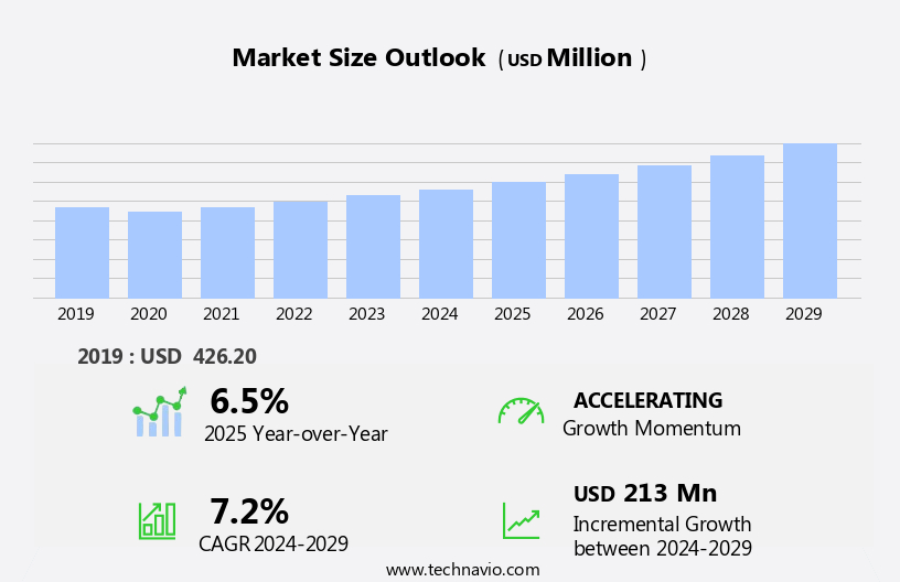
The semiconductor photoresist stripping market size is forecast to increase by USD 213 million, at a CAGR of 7.2% between 2024 and 2029.
- The market is driven by the continuous advancements in stripping equipment technology, enabling efficient and effective photoresist removal from semiconductor wafers. This market growth is further fueled by the increasing demand for multi-layered devices and complex 3D structures in the semiconductor industry. However, challenges persist in ensuring seamless process integration and maintaining uniformity throughout the photoresist stripping process. These challenges necessitate ongoing research and development efforts to address the complexities of stripping advanced photoresist layers while minimizing damage to underlying structures.
- Companies seeking to capitalize on this market's opportunities must stay abreast of technological advancements and invest in innovative solutions to overcome the challenges associated with photoresist stripping in the semiconductor industry.
What will be the Size of the Semiconductor Photoresist Stripping Market during the forecast period?
Explore in-depth regional segment analysis with market size data - historical 2019-2023 and forecasts 2025-2029 - in the full report.
Request Free Sample
The market is a dynamic and evolving landscape, integral to the intricacies of semiconductor manufacturing. This market plays a pivotal role in various stages of wafer fabrication, from substrate preparation to yield improvement. Photoresist stripping, a crucial process in semiconductor manufacturing, enables the removal of photoresist layers post-etching, ensuring critical dimension and etch profile accuracy. Throughput optimization is a continuous pursuit in semiconductor manufacturing, with photoresist stripping contributing significantly. EUV lithography, a cutting-edge technology, necessitates advanced photoresist stripping techniques for efficient and effective etch rate control. Etch depth uniformity and linewidth roughness are critical factors influencing market dynamics, with immersion lithography and plasma etching playing essential roles.
Equipment maintenance, process control, and environmental compliance are paramount in this market. Statistical process control, contamination control, and cleanroom technology are employed to maintain process capability and minimize defect density. Photoresist spin coating and resist coating optimization are essential for achieving high-resolution patterns. Process optimization techniques, such as plasma power management and solvent type selection, impact photoresist stripping efficiency. Surface chemistry and material science advancements continue to unfold, driving market growth. Cost reduction and safety regulations are key considerations, with ultrasonic cleaning and solvent cleaning offering cost-effective solutions. Semiconductor manufacturing's intricate nature necessitates ongoing research and development in photoresist stripping technologies.
The market's continuous evolution reflects the interconnectedness of its components: etch rate, plasma gas selection, optical proximity correction, dry etching, thin film deposition, and residue removal. The market's dynamism is a testament to its indispensable role in the semiconductor industry.
How is this Semiconductor Photoresist Stripping Industry segmented?
The semiconductor photoresist stripping industry research report provides comprehensive data (region-wise segment analysis), with forecasts and estimates in "USD million" for the period 2025-2029, as well as historical data from 2019-2023 for the following segments.
- Type
- Positive
- Negative
- Application
- Integrated circuit manufacturing
- Wafer level packaging
- Method
- Wet stripping
- Dry stripping
- Material
- Aqueous cleaning materials
- Semi-aqueous cleaning materials
- Technique
- Wet clean
- Strip
- Etch
- Geography
- North America
- US
- Canada
- Europe
- France
- Germany
- Italy
- UK
- APAC
- China
- India
- Japan
- South Korea
- Rest of World (ROW)
- North America
By Type Insights
The positive segment is estimated to witness significant growth during the forecast period.
In the intricate world of semiconductor manufacturing, the process of photoresist stripping plays a pivotal role in optimizing throughput and enhancing yield. Once patterns are transferred onto a silicon wafer through photolithography using photomasks, the unexposed photoresist material must be removed to unveil the patterned areas for subsequent processing. Positive photoresist, which acts as a mask during etching, is essential for selectively removing materials and creating circuit patterns and features. After the etching process, the unexposed areas of positive photoresist are stripped away, revealing the etched features and enabling precise pattern transfer. Moreover, photoresist stripping is crucial for removing residues left behind after etching or other processing steps.
These residues, if not addressed, can hinder subsequent processes, negatively impacting device performance and yield. The efficiency of photoresist stripping significantly influences manufacturing efficiency, as it directly impacts the overall semiconductor manufacturing process. Material science plays a vital role in photoresist stripping, with factors like etch depth, etch rate, and critical dimension influencing the effectiveness of the process. Environmental compliance is another essential consideration, as various solvents and ultrasonic or plasma etching techniques are used for stripping. Process control, statistical process control, and contamination control are also crucial to ensure consistent, high-quality results. Photoresist stripping techniques include immersion lithography, wet etching, and dry etching, with plasma etching and plasma gas playing a significant role in optimizing the process.
Safety regulations, such as those related to solvent type and handling, are essential to ensure a safe working environment. In the realm of integrated circuit fabrication, the importance of photoresist stripping is evident, as it sets the stage for subsequent processing steps and ultimately impacts the final product's performance and yield.

The Positive segment was valued at USD 340.90 million in 2019 and showed a gradual increase during the forecast period.
Regional Analysis
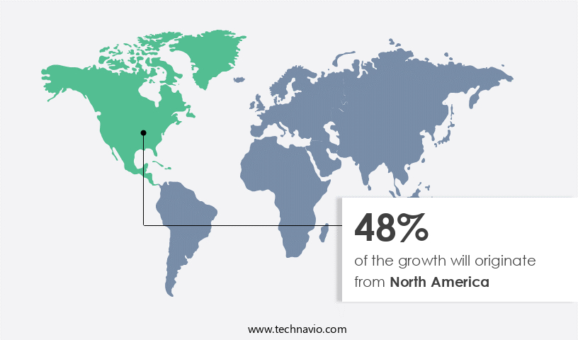
North America is estimated to contribute 48% to the growth of the global market during the forecast period.Technavio’s analysts have elaborately explained the regional trends and drivers that shape the market during the forecast period.
In North America, the market experiences steady growth due to the presence of a substantial number of semiconductor manufacturing facilities, primarily in the US. The region's thriving semiconductor industry, fueled by demand from sectors like electronics, automotive, and telecommunications, propels market expansion. Advanced semiconductor technology developments, such as smaller feature sizes, increased circuit densities, and innovative materials, necessitate advanced photoresist stripping solutions. Semiconductor manufacturers in North America invest in advanced technologies to maintain competitiveness, thereby driving market growth. The increasing demand for sophisticated semiconductor devices, including microprocessors, memory chips, and sensors, is driven by trends like artificial intelligence, the Internet of Things (IoT), and 5G technology.
Throughput optimization, equipment maintenance, and yield improvement are essential considerations in semiconductor manufacturing. EUV lithography and immersion lithography, critical dimensions and etch profiles, substrate preparation, and post-etch cleaning are integral parts of the manufacturing process. Photoresist spin coating and resist removal, process control, and material science are essential for maintaining process capability and defect density. Contamination control, cleanroom technology, and process optimization are crucial for ensuring edge roughness and surface chemistry. Cost reduction, safety regulations, and environmental compliance are significant factors influencing the market. Ultrasonic cleaning, solvent cleaning, plasma etching, and thin film deposition are essential techniques used in semiconductor manufacturing.
Chemical mechanical planarization, wet etching, and deep UV lithography are also integral to the process. The market is characterized by continuous advancements in technology, with resolution enhancement techniques and plasma power playing a vital role. Silicon wafer waste management and hard baking are essential aspects of semiconductor manufacturing. Defect inspection and plasma gas optimization are crucial for maintaining manufacturing efficiency.
Market Dynamics
Our researchers analyzed the data with 2024 as the base year, along with the key drivers, trends, and challenges. A holistic analysis of drivers will help companies refine their marketing strategies to gain a competitive advantage.
The market is a critical segment in the global semiconductor industry, focusing on the removal of photoresist layers from silicon wafers post-lithography process. This market encompasses various technologies, including wet and dry stripping methods, plasma-based techniques, and chemical solutions. Key players in this market prioritize innovation to address challenges such as high processing costs, environmental concerns, and the need for higher productivity and efficiency. Advanced technologies like nanotechnology, organic photochemistry, and biomimetic approaches are shaping the semiconductor photoresist stripping landscape. Market trends include the integration of automation and robotics, the adoption of green and eco-friendly stripping solutions, and the increasing demand for high-precision and high-throughput processes. Semiconductor manufacturers, research institutes, and equipment suppliers are actively collaborating to develop next-generation photoresist stripping solutions that cater to the evolving demands of the semiconductor industry.
What are the key market drivers leading to the rise in the adoption of Semiconductor Photoresist Stripping Industry?
- The market's growth is primarily attributed to advancements in stripping equipment technology.
- Semiconductor photoresist stripping is a critical process in the semiconductor industry, involving the selective removal of photoresist material from wafers after lithography. Advanced stripping equipment is essential to meet the increasing demand for high-volume production. These systems offer enhanced manufacturing efficiency and productivity through improved automation, faster cycle times, and optimized process recipes. Modern stripping equipment features multi-step and multi-chamber configurations, enabling sequential processing steps such as wet stripping, plasma etching, and wafer cleaning, within a single platform. This minimizes wafer handling and cycle time while maximizing process control and uniformity. Advancements in stripping technology enable selective removal of photoresist material from specific regions of semiconductor wafers, such as patterned areas or device layers.
- Wet etching and plasma etching are common methods used for photoresist stripping. Safety regulations, including those related to particle counting and strip temperature, are crucial considerations in the design and operation of these systems. Thin film deposition and residue removal are also important processes that may be integrated into the stripping equipment. Overall, the market is driven by the need for increased manufacturing efficiency, productivity, and selectivity in semiconductor fabrication processes.
What are the market trends shaping the Semiconductor Photoresist Stripping Industry?
- The increasing demand for multi-layered devices and complex 3D structures represents a significant market trend. Professionals anticipate continued growth in this area due to its potential for enhanced functionality and advanced design.
- In the intricate world of semiconductor manufacturing, the demand for precise and selective photoresist stripping processes is on the rise. With the advent of multi-layered devices and 3D structures, such as FinFET transistors and 3D NAND flash memory, the need for advanced stripping solutions is becoming increasingly crucial. These complex semiconductor architectures necessitate selective stripping processes to remove photoresist from specific regions or layers while preserving underlying materials. Advanced photoresist stripping equipment and techniques, like plasma etching and wet stripping, play a pivotal role in achieving this selectivity. These methods enable the removal of photoresist material with high precision and uniformity, thereby supporting the fabrication of multi-layered semiconductor devices with intricate architectures.
- Throughput optimization in wafer fabrication processes is another critical factor driving the demand for advanced photoresist stripping solutions. Efficient stripping processes can significantly reduce equipment downtime for maintenance and post-etch cleaning, leading to yield improvement and linewidth roughness reduction. Immersion lithography and EUV lithography, which are essential for manufacturing advanced semiconductor devices, rely heavily on reliable and effective photoresist stripping processes. Overall, the market dynamics of photoresist stripping solutions are shaped by the continuous pursuit of higher performance, functionality, and cost-effectiveness in semiconductor manufacturing.
What challenges does the Semiconductor Photoresist Stripping Industry face during its growth?
- The integration and uniformity of photoresist stripping processes, which encompass concerns related to industry growth, pose a significant challenge for the semiconductor industry.
- Semiconductor manufacturing involves intricate processes, including photoresist stripping, which plays a crucial role in determining wafer quality and overall yield. Variability in stripping conditions, equipment performance, and wafer characteristics can lead to inconsistent results, causing yield loss, reduced device performance, and increased manufacturing costs. Different semiconductor materials and device structures necessitate specific photoresist stripping chemistries and processes. Ensuring uniform stripping results across various material types, such as silicon, silicon dioxide, and metal films, while maintaining material integrity and device performance is a significant challenge. Environmental compliance, including contamination control in cleanroom technology, is essential during photoresist stripping. Techniques like ultrasonic cleaning and solvent cleaning are commonly used for process optimization.
- Material science and resolution enhancement techniques are integral to achieving consistent stripping results. Process control, including etch rate and edge roughness, is critical to ensure compatibility with other process steps like lithography and etching. The choice of solvent type and resist coating also influences the stripping process's effectiveness. Maintaining consistency and repeatability in photoresist stripping results across multiple tools and equipment platforms is essential for high-volume semiconductor manufacturing.
Exclusive Customer Landscape
The semiconductor photoresist stripping market forecasting report includes the adoption lifecycle of the market, covering from the innovator’s stage to the laggard’s stage. It focuses on adoption rates in different regions based on penetration. Furthermore, the semiconductor photoresist stripping market report also includes key purchase criteria and drivers of price sensitivity to help companies evaluate and develop their market growth analysis strategies.

Customer Landscape
Key Companies & Market Insights
Companies are implementing various strategies, such as strategic alliances, semiconductor photoresist stripping market forecast, partnerships, mergers and acquisitions, geographical expansion, and product/service launches, to enhance their presence in the industry.
Advanced Energy Industries Inc. - The company specializes in providing advanced semiconductor photoresist stripping solutions, including Centris SYM3 Y Etch, Centura Etch, and Centura Tetra Z Photomask Etch. These innovative offerings ensure efficient and effective photoresist removal, enhancing overall semiconductor manufacturing processes. The company's commitment to research and development results in continuous improvement and expansion of its product portfolio, addressing the evolving needs of the global semiconductor industry.
The industry research and growth report includes detailed analyses of the competitive landscape of the market and information about key companies, including:
- Advanced Energy Industries Inc.
- Allwin21 Corp.
- Applied Materials Inc.
- Brewer Science Inc.
- Brinnovate
- EV Group
- Hitachi Ltd.
- Lam Research Corp.
- Mattson Technology Inc.
- Merck KGaA
- MT Systems Inc.
- Nordson Corp.
- Oxford Instruments plc
- PSK Inc.
- Samco Inc.
- Screen Holdings Co. Ltd
- TBS Holdings Inc.
- Trymax Semiconductor Equipment B.V.
- Ulvac Inc.
Qualitative and quantitative analysis of companies has been conducted to help clients understand the wider business environment as well as the strengths and weaknesses of key industry players. Data is qualitatively analyzed to categorize companies as pure play, category-focused, industry-focused, and diversified; it is quantitatively analyzed to categorize companies as dominant, leading, strong, tentative, and weak.
Recent Development and News in Semiconductor Photoresist Stripping Market
- In January 2024, Intel Corporation announced the launch of its new photoresist stripping solution, called Intel Oxi-Gone, which utilizes an advanced oxide removal technology, reducing water usage by up to 90% compared to traditional methods. (Intel Press Release)
- In March 2024, Tokyo Electron Limited and ASML Holding NV entered into a strategic partnership to jointly develop and commercialize next-generation photoresist stripping technologies, aiming to improve productivity and reduce costs for semiconductor manufacturers. (ASML Press Release)
- In May 2024, Lam Research Corporation completed the acquisition of KLA-Tencor Corporation's photoresist strip business, expanding its portfolio and strengthening its position in the semiconductor equipment market. The deal was valued at approximately USD4.7 billion. (Lam Research Press Release)
- In February 2025, the European Union approved a â¬1.8 billion (USD2 billion) funding program to support the development and manufacturing of advanced semiconductor technologies, including investments in photoresist stripping solutions, to reduce Europe's dependence on imports and bolster its semiconductor industry. (European Commission Press Release)
Research Analyst Overview
- The market is experiencing significant advancements, driven by the integration of automated optical inspection (AOI) and automated defect review (ADR) systems. Chemical amplified resist, such as negative and positive photoresists, plays a crucial role in this process, enabling higher sensitivity and yield enhancement. In-line inspection systems and off-line inspection systems ensure material characterization and process monitoring, while safety protocols and energy efficiency are essential considerations. Process simulation, resist spin speed, and viscosity optimization contribute to waste minimization and development time reduction.
- High-k and low-k dielectrics, along with advanced materials, are essential for smart manufacturing and real-time monitoring. Statistical analysis and automation systems facilitate process characterization and defect classification. Exposure dose and process monitoring tools ensure quality control, while water recycling and VOC emissions reduction are critical for environmental impact assessment. Process simulation and data analytics are key to improving process efficiency and enhancing overall manufacturing performance.
Dive into Technavio’s robust research methodology, blending expert interviews, extensive data synthesis, and validated models for unparalleled Semiconductor Photoresist Stripping Market insights. See full methodology.
|
Market Scope |
|
|
Report Coverage |
Details |
|
Page number |
228 |
|
Base year |
2024 |
|
Historic period |
2019-2023 |
|
Forecast period |
2025-2029 |
|
Growth momentum & CAGR |
Accelerate at a CAGR of 7.2% |
|
Market growth 2025-2029 |
USD 213 million |
|
Market structure |
Fragmented |
|
YoY growth 2024-2025(%) |
6.5 |
|
Key countries |
US, Canada, China, Germany, Japan, France, India, South Korea, Italy, and UK |
|
Competitive landscape |
Leading Companies, Market Positioning of Companies, Competitive Strategies, and Industry Risks |
What are the Key Data Covered in this Semiconductor Photoresist Stripping Market Research and Growth Report?
- CAGR of the Semiconductor Photoresist Stripping industry during the forecast period
- Detailed information on factors that will drive the growth and forecasting between 2025 and 2029
- Precise estimation of the size of the market and its contribution of the industry in focus to the parent market
- Accurate predictions about upcoming growth and trends and changes in consumer behaviour
- Growth of the market across North America, Europe, APAC, South America, and Middle East and Africa
- Thorough analysis of the market’s competitive landscape and detailed information about companies
- Comprehensive analysis of factors that will challenge the semiconductor photoresist stripping market growth of industry companies
We can help! Our analysts can customize this semiconductor photoresist stripping market research report to meet your requirements.
 RIA -
RIA - 
