
Sputtering Equipment Market Size 2024-2028
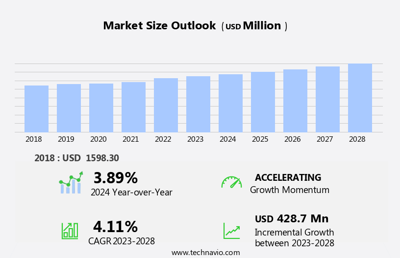
The sputtering equipment market size is forecast to increase by USD 428.7 million, at a CAGR of 4.11% between 2023 and 2028.
- The market is experiencing significant shifts due to the expanding application scope in advanced technology sectors. Notably, the increasing demand for Internet of Things (IoT) devices is driving market growth. Sputtering equipment plays a crucial role in the manufacturing process of various IoT components, such as sensors and microelectronics. However, the market faces challenges as well. The declining demand for traditional storage media like CDs, DVDs, and Blu-ray discs poses a threat to the market's growth. Furthermore, the high capital investment and complex nature of sputtering equipment may deter small-scale and emerging companies from entering the market.
- Additionally, the need for continuous innovation to meet evolving technology requirements adds to the market's challenges. Companies must navigate these obstacles while capitalizing on the opportunities presented by the IoT sector to maintain a competitive edge.
What will be the Size of the Sputtering Equipment Market during the forecast period?
Explore in-depth regional segment analysis with market size data - historical 2018-2022 and forecasts 2024-2028 - in the full report.
Request Free Sample
The market is characterized by its continuous evolution and dynamic nature, with ongoing advancements and applications across various sectors. Sputtering systems, utilizing ceramic targets, rotary vane pumps, and sputtering targets, are integral components in thin film deposition processes for diverse industries. Yield optimization and cost analysis are key considerations, with optical coatings and ion beam sputtering playing essential roles in enhancing performance and efficiency. Automation systems and regulatory compliance are increasingly important, ensuring seamless integration of power supplies, dc sputtering, and process control software. In the realm of semiconductor manufacturing, chamber design and process optimization are paramount, with reactive sputtering and plasma etching contributing significantly to the production of advanced materials.
Environmental impact, pressure sensors, and vacuum pumps are essential aspects of sputtering equipment, with turbomolecular pumps and cooling systems ensuring optimal conditions for deposition. Target material selection, cleaning, and manufacturing processes are crucial for maintaining quality and consistency. Process control software, data acquisition systems, and safety regulations are integral to ensuring efficient and reliable sputtering operations. Defect analysis, deposition rate, film uniformity, and surface roughness are critical factors in evaluating the performance of sputtering systems. The market for sputtering equipment is vast and diverse, encompassing applications in medical devices, solar cells, compound targets, and more. As material science continues to advance, the demand for innovative sputtering solutions will persist, driving the ongoing evolution of this dynamic market.
How is this Sputtering Equipment Industry segmented?
The sputtering equipment industry research report provides comprehensive data (region-wise segment analysis), with forecasts and estimates in "USD million" for the period 2024-2028, as well as historical data from 2018-2022 for the following segments.
- Type
- Reactive sputtering
- Magnetron sputtering
- Co-sputtering
- Application
- Solar energy
- Display
- Data storage
- Semiconductor
- Others
- Geography
- North America
- US
- APAC
- China
- Japan
- South Korea
- Taiwan
- Rest of World (ROW)
- North America
By Type Insights
The reactive sputtering segment is estimated to witness significant growth during the forecast period.
Sputtering, a physical vapor deposition (PVD) technique, is widely used for creating thin-film coatings in various industries. The process involves bombarding a target made of the desired material with an inert gas, typically argon, creating a vapor cloud. Ionization of the non-inert gas in the chamber causes a chemical reaction, resulting in the formation of the deposited film. The market is experiencing significant growth due to the increasing adoption of micro-electromechanical systems (MEMS) sensors. MEMS technology, which combines mechanical and electrical components in miniaturized devices, is gaining popularity in the electronics industry. Sputtering is an essential process in MEMS manufacturing, driving the demand for advanced sputtering systems.
Material science plays a crucial role in sputtering, with compound targets used to create complex thin films. Magnetron sputtering, a common sputtering technique, enables high deposition rates and excellent film uniformity. Process optimization, including substrate heating, target erosion control, and process gas control, is essential for achieving high-quality coatings. Medical devices, solar cells, and semiconductor manufacturing are major industries utilizing sputtering technology. Regulatory compliance, safety regulations, and waste management are critical considerations in these applications. Automation systems, power supplies, and cooling systems are integral components of modern sputtering systems. Cost analysis, including target material selection and manufacturing, cooling systems, and vacuum pumps, significantly impacts the overall cost of sputtering systems.
Ion beam sputtering and reactive sputtering are advanced techniques used for specific applications, such as optical coatings and defect analysis. Process control software, data acquisition systems, and maintenance procedures ensure optimal yield and process efficiency. Environmental impact, including the use of vacuum chambers and turbomolecular pumps, is an ongoing concern in the sputtering industry. Thickness monitors, surface roughness, and adhesion testing are essential quality control measures. In the semiconductor manufacturing sector, sputtering systems are used for depositing thin films in the production of integrated circuits. Chamber design, deposition rate, and film uniformity are critical factors in semiconductor manufacturing.
X-ray reflectivity (xrr) and other characterization techniques are used to evaluate the quality of the deposited films. Sputtering targets, including ceramic, metal, and alloy targets, are essential components of sputtering systems. Target manufacturing, target cleaning, and target material selection are crucial aspects of target production. Quality control, data storage, and safety regulations are essential considerations in target manufacturing processes.
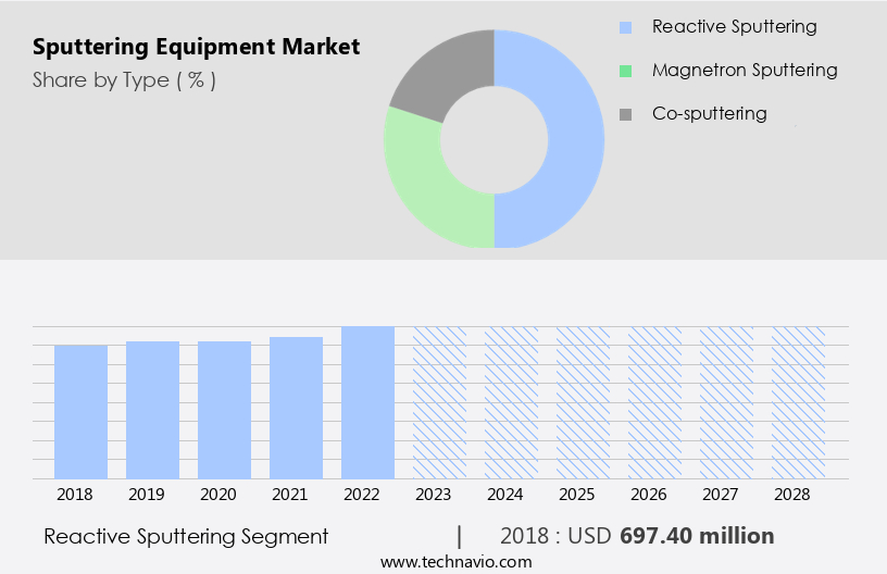
The Reactive sputtering segment was valued at USD 697.40 million in 2018 and showed a gradual increase during the forecast period.
Regional Analysis
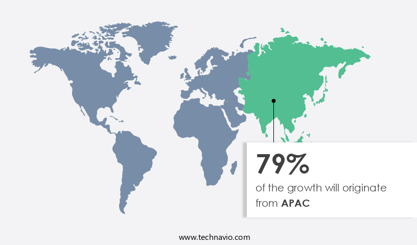
APAC is estimated to contribute 79% to the growth of the global market during the forecast period. Technavio's analysts have elaborately explained the regional trends and drivers that shape the market during the forecast period.
The market is witnessing significant growth due to the increasing demand for thin film deposition in various industries. RF Sputtering and DC Sputtering are popular techniques used for thin film deposition, offering benefits such as high deposition rates, film uniformity, and excellent film quality. Film stress measurement is crucial in ensuring the quality of thin films, and plasma diagnostics plays a vital role in monitoring the plasma conditions during the deposition process. Sputtering systems are used in various applications, including medical devices, solar cells, and semiconductor manufacturing. Compound targets and alloy targets are widely used in the production of optical coatings and magnetic films.
Material science research and development in the field of sputtering technology are driving innovation, leading to the development of new target materials and chamber designs. Cooling systems and vacuum pumps are essential components of sputtering systems, ensuring efficient and stable operation. Cost analysis is a critical factor in the selection of sputtering equipment, with rotary vane pumps and turbomolecular pumps offering cost-effective solutions. Automation systems and process control software are increasingly being adopted to optimize yield and improve process consistency. Regulatory compliance is a significant consideration in the selection of sputtering equipment, with safety regulations and waste management being key concerns.
Magnetron sputtering and reactive sputtering are popular techniques used in the production of high-performance films. Defect analysis and deposition rate monitoring are essential for maintaining high-quality films and improving process efficiency. Process optimization and maintenance procedures are crucial for ensuring the longevity and reliability of sputtering equipment. Process gas control and data acquisition systems enable real-time monitoring and analysis of the deposition process, improving process consistency and reducing downtime. Ion beam sputtering and plasma etching are advanced techniques used for surface modification and material processing. The APAC region is a major market for sputtering equipment due to the presence of major consumer electronics manufacturers, automotive manufacturers, and solar cell manufacturers in the region.
The abundant availability of raw materials and low labor costs make it an attractive destination for companies looking to set up production centers. The region's presence of many OEMs and research institutions is driving innovation and technological advancements in the field of sputtering technology.
Market Dynamics
Our researchers analyzed the data with 2023 as the base year, along with the key drivers, trends, and challenges. A holistic analysis of drivers will help companies refine their marketing strategies to gain a competitive advantage.
What are the key market drivers leading to the rise in the adoption of Sputtering Equipment Industry?
- The growth of the piezoelectric MEMS (Micro-Electromechanical Systems) market is primarily driven by the increasing demand and advancements in this technology. These miniature devices, which convert mechanical energy into electrical energy, offer numerous applications in various industries, including automotive, healthcare, and consumer electronics. As a result, the market for piezoelectric MEMS is experiencing significant expansion and innovation.
- Thin film deposition through RF sputtering is a critical technology in various industries, including medical devices, solar cells, and material science. RF sputtering utilizes plasma to deposit thin films on substrates, enabling the production of high-quality coatings with excellent adhesion and uniformity. The market for RF sputtering equipment is driven by the increasing demand for advanced materials and components in numerous applications. Film stress measurement and target erosion are essential considerations in RF sputtering. Plasma diagnostics and substrate heating are crucial process parameters that influence the quality of the deposited films. Compound targets and multi-target sputtering enhance the versatility of RF sputtering systems, allowing the deposition of various materials in a single process.
- The cost analysis of RF sputtering systems is an essential factor in their adoption. Cooling systems and pulsed DC sputtering are alternative techniques that offer cost savings while maintaining the desired film quality. In the medical devices sector, RF sputtering is used for coating stents, implants, and sensors, while in solar cells, it is employed for producing thin films for photovoltaic applications. Thin film deposition through RF sputtering is a vital technology in material science, with applications ranging from MEMS manufacturing to solar cells and medical devices. The increasing trend towards miniaturization and the demand for high-performance materials are driving the growth of the RF the market.
What are the market trends shaping the Sputtering Equipment Industry?
- The increasing demand for Internet of Things (IoT) devices represents a significant market trend in the professional and knowledgeable technology sector. IoT devices are becoming increasingly popular due to their ability to connect and exchange data in real time, enhancing efficiency and productivity.
- The semiconductor industry is experiencing significant growth due to the increasing adoption of Internet of Things (IoT) technology. IoT devices rely heavily on semiconductor sensor technology, making semiconductor inspection systems essential for producing sensors of superior quality. IoT enables devices to collect, record, and transmit data in real-time without human intervention. The advancements in telecommunication standards, such as 3G/4G/5G and wired communication standards, have accelerated the proliferation of IoT devices. Sputtering systems play a pivotal role in the semiconductor manufacturing process. These systems utilize sputtering targets, often made of ceramic materials, to deposit thin films on substrates.
- Ion beam sputtering is a popular technique used for depositing high-quality optical coatings. Sputtering equipment requires robust rotary vane pumps, power supplies, and automation systems for yield optimization. Chamber design and process control software are also crucial for ensuring regulatory compliance. DC sputtering is another technique used for depositing thin films. The target material is subjected to a high-energy plasma to create ions that deposit on the substrate. The market for sputtering equipment is expected to grow due to the increasing demand for advanced semiconductor technologies and the need for higher performance and reliability.
What challenges does the Sputtering Equipment Industry face during its growth?
- The decline in consumer demand for CDs, DVDs, and Blu-ray discs poses a significant challenge to the industry's growth trajectory.
- Sputtering equipment plays a crucial role in the deposition of thin films of metal, such as aluminum or gold, for the production of CDs, DVDs, and Blu-ray discs. Magnetron sputtering is a widely used technique in this process, which employs magnets behind the negative cathode to accelerate electrons towards the target material, increasing deposition rates. However, the declining demand for optical discs due to digital media's growing popularity is adversely impacting the market growth for magnetron sputtering. Moreover, advanced sputtering techniques like reactive sputtering, bias sputtering, and remote plasma sputtering are gaining traction for their ability to deposit high-quality films with improved defect analysis, deposition rate, film uniformity, and process optimization.
- These techniques require precise process gas control, pressure sensors, and maintenance procedures for efficient waste management. Environmental concerns have led to the development of eco-friendly sputtering equipment, which uses less energy and generates minimal waste. Pressure sensors and vacuum pumps are essential components of these systems, ensuring optimal process conditions and reducing energy consumption. Turbomolecular pumps are commonly used for high-vacuum applications due to their ability to pump gases efficiently and maintain a stable vacuum environment. The market is driven by the demand for advanced thin film technologies and the need for eco-friendly solutions.
- Market companies must focus on continuous process optimization, waste management, and energy efficiency to remain competitive in this market.
Exclusive Customer Landscape
The sputtering equipment market forecasting report includes the adoption lifecycle of the market, covering from the innovator's stage to the laggard's stage. It focuses on adoption rates in different regions based on penetration. Furthermore, the sputtering equipment market report also includes key purchase criteria and drivers of price sensitivity to help companies evaluate and develop their market growth analysis strategies.

Customer Landscape
Key Companies & Market Insights
Companies are implementing various strategies, such as strategic alliances, sputtering equipment market forecast, partnerships, mergers and acquisitions, geographical expansion, and product/service launches, to enhance their presence in the industry.
Angstrom Science Inc. - The company specializes in ONYX magnetron sputtering cathodes featuring intricate multi-cathode cluster assemblies, ideally suited for system upgrades and retrofit applications.
The industry research and growth report includes detailed analyses of the competitive landscape of the market and information about key companies, including:
- Angstrom Science Inc.
- Applied Materials Inc.
- Buhler AG
- Canon Inc.
- Denton Vacuum
- Guangdong HuiCheng Vacuum Technology Co. Ltd.
- Impact Coatings AB
- Intevac Inc.
- IZOVAC PHOTONICS
- Kobe Steel Ltd.
- KOLZER SRL
- Kurt J Lesker Co.
- OC Oerlikon Corp. AG
- Semicore Equipment Inc.
- Singulus Technologies AG
- Tokyo Electron Ltd.
- Ulvac Inc.
- Vacuum Techniques Pvt. Ltd.
- Veeco Instruments Inc.
- Vergason Technology Inc.
Qualitative and quantitative analysis of companies has been conducted to help clients understand the wider business environment as well as the strengths and weaknesses of key industry players. Data is qualitatively analyzed to categorize companies as pure play, category-focused, industry-focused, and diversified; it is quantitatively analyzed to categorize companies as dominant, leading, strong, tentative, and weak.
Recent Development and News in Sputtering Equipment Market
- In January 2024, Tokyo Electron Limited, a leading manufacturer of semiconductor production equipment, announced the launch of a new magnetron sputtering system, the JC9D2500GRA, designed for high-volume manufacturing of advanced semiconductor devices (Tokyo Electron Press Release, 2024). This system reportedly offers improved throughput and uniformity, addressing the increasing demand for smaller and more complex semiconductor features.
- In March 2024, Applied Materials, Inc. and Lam Research Corporation, two major players in the semiconductor equipment industry, announced a strategic collaboration to develop and commercialize next-generation etch and deposition technologies (Applied Materials Press Release, 2024). This partnership aims to accelerate the development of advanced semiconductor manufacturing processes, enabling the production of smaller, more efficient, and cost-effective devices.
- In May 2024, Veeco Instruments Inc. completed the acquisition of Ulvac, Inc.'s sputtering business, expanding Veeco's product portfolio and enhancing its position in the market (Veeco Instruments Press Release, 2024). This acquisition reportedly strengthens Veeco's presence in the Asian market and provides access to Ulvac's advanced sputtering technologies and customer base.
- In February 2025, ASML Holding NV, a leading provider of photolithography equipment for the semiconductor industry, announced the successful deployment of its latest extreme ultraviolet (EUV) lithography system, the Twinscan Xtrencher 1900Gi, at a major semiconductor manufacturer (ASML Holding NV Press Release, 2025). This system, which incorporates advanced sputtering technology for EUV mask production, marks a significant step forward in the mass production of next-generation semiconductor devices.
Research Analyst Overview
- The market encompasses various technologies used for surface modification and thin film deposition. Key processes include post-treatment techniques such as plasma cleaning, ion plating, and in-situ analysis. Dry etching methods like reactive ion etching and laser ablation are gaining traction, while wet etching continues to dominate certain applications. Inkjet printing and spin coating are essential for substrate preparation in advanced manufacturing processes. Surface analysis tools like X-ray diffraction (XRD) and surface treatment methods such as ultrasonic cleaning and sol-gel processing are integral to ensuring high-quality thin films. Pre-treatment optimization is crucial for effective coating adhesion, with techniques like chemical cleaning and dip coating playing significant roles.
- Etching techniques, including plasma processing and thermal evaporation, are essential for creating intricate structures and patterns. Roll-to-roll processing and process monitoring technologies enable mass production and improve overall efficiency in the industry. Developments in cleaning processes, such as plasma cleaning and ultrasonic cleaning, are driving innovation in the market. The integration of these advanced technologies enhances the overall quality and reliability of thin films and coatings, making them indispensable in various industries.
Dive into Technavio's robust research methodology, blending expert interviews, extensive data synthesis, and validated models for unparalleled Sputtering Equipment Market insights. See full methodology.
|
Market Scope |
|
|
Report Coverage |
Details |
|
Page number |
183 |
|
Base year |
2023 |
|
Historic period |
2018-2022 |
|
Forecast period |
2024-2028 |
|
Growth momentum & CAGR |
Accelerate at a CAGR of 4.11% |
|
Market growth 2024-2028 |
USD 428.7 million |
|
Market structure |
Fragmented |
|
YoY growth 2023-2024(%) |
3.89 |
|
Key countries |
China, Taiwan, Japan, US, and South Korea |
|
Competitive landscape |
Leading Companies, Market Positioning of Companies, Competitive Strategies, and Industry Risks |
What are the Key Data Covered in this Sputtering Equipment Market Research and Growth Report?
- CAGR of the Sputtering Equipment industry during the forecast period
- Detailed information on factors that will drive the growth and forecasting between 2024 and 2028
- Precise estimation of the size of the market and its contribution of the industry in focus to the parent market
- Accurate predictions about upcoming growth and trends and changes in consumer behaviour
- Growth of the market across APAC, North America, Europe, South America, and Middle East and Africa
- Thorough analysis of the market's competitive landscape and detailed information about companies
- Comprehensive analysis of factors that will challenge the sputtering equipment market growth of industry companies
We can help! Our analysts can customize this sputtering equipment market research report to meet your requirements.
 RIA -
RIA - 
