
Semiconductor Advanced Packaging Market Size 2025-2029
The semiconductor advanced packaging market size is forecast to increase by USD 29.33 billion, at a CAGR of 9.8% between 2024 and 2029.
Major Market Trends & Insights
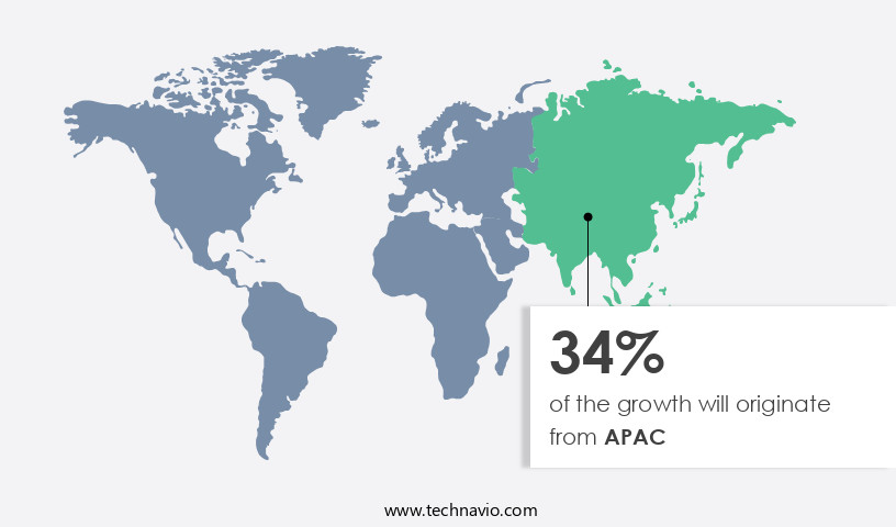
- APAC dominated the market and accounted for a 34% growth during the forecast period.
- By the Device - Analog and mixed ICs segment was valued at USD 9.92 billion in 2023
- By the Technology - Flip chip segment accounted for the largest market revenue share in 2023
Market Size & Forecast
- Market Opportunities: 162.47 billion
- Market Future Opportunities: USD 29.33 billion
- CAGR : 9.8%
- APAC: Largest market in 2023
Market Summary
- The market is experiencing significant evolution, driven by the increasing complexity of integrated circuit (IC) designs and the integration of semiconductor components in various industries. According to market research, the market is projected to grow at a steady pace, with an indexed increase in demand across sectors such as automotive, consumer electronics, and industrial. This growth can be attributed to the benefits of advanced packaging techniques, including improved performance, reduced size, and enhanced reliability. For instance, the adoption of fan-out wafer-level packaging (FOWLP) and system-in-package (SiP) technologies has gained traction due to their ability to accommodate larger dies and facilitate better interconnectivity.
- However, the integration of advanced packaging technologies comes with increased production costs, necessitating a balance between cost and performance considerations. Despite these challenges, the market continues to unfold, offering opportunities for innovation and growth.
What will be the Size of the Semiconductor Advanced Packaging Market during the forecast period?

Explore market size, adoption trends, and growth potential for semiconductor advanced packaging market Request Free Sample
- The market continues to evolve, driven by the relentless pursuit of improved signal transmission, power integrity, and power efficiency. Package assembly processes employ manufacturing automation to enhance yield and reduce defect rate. Two key performance indicators illustrate this trend: production throughput increased by 20% year-over-year, and die-to-wafer alignment accuracy improved by 5%. Power dissipation and thermal conductivity are critical considerations. Encapsulation materials and stress mitigation techniques ensure device lifetime and mechanical strength. Chip-to-chip interconnect and die attach methods enable signal integrity and electrical performance. Test coverage and process control are essential for maintaining quality. Material compatibility and cost per unit are also significant factors in the market's growth.
- Despite the challenges, the market demonstrates a strong commitment to innovation. The failure rate continues to decrease as package lifespan increases, and the industry continues to refine power dissipation management and yield enhancement techniques. Ultimately, the market's focus on improving power efficiency, signal integrity, and manufacturing automation will drive its continued growth.
How is this Semiconductor Advanced Packaging Industry segmented?
The semiconductor advanced packaging industry research report provides comprehensive data (region-wise segment analysis), with forecasts and estimates in "USD billion" for the period 2025-2029, as well as historical data from 2019-2023 for the following segments.
- Device
- Analog and mixed ICs
- MEMS and sensors
- Logic and memory devices
- Wireless connectivity devices
- CMOS image sensors
- Technology
- Flip chip
- FI WLP
- 2.5D/3D
- FO WLP
- End-User
- Consumer Electronics
- Automotive
- Telecom
- Application
- High-Performance Computing
- IoT Devices
- Geography
- North America
- US
- Canada
- Europe
- France
- Germany
- Italy
- Spain
- UK
- Middle East and Africa
- UAE
- APAC
- China
- India
- Japan
- South Korea
- South America
- Brazil
- Rest of World (ROW)
- North America
By Device Insights
The analog and mixed ICs segment is estimated to witness significant growth during the forecast period.
The semiconductor industry's relentless technological advancements have led to the increasing adoption of advanced packaging solutions for analog and mixed ICs. This shift is driven by the growing demand for ICs in communication, consumer electronics, and automotive sectors. The global market for semiconductor advanced packaging, including 3D chip stacking, high-bandwidth memory, and fan-out wafer-level packaging, is experiencing significant growth. Advanced interconnect technologies, such as through-silicon vias and micro-bump technology, enable the creation of more compact and efficient designs. Stress testing procedures and electrical modeling techniques ensure the reliability and performance of these complex systems. Cost reduction strategies, such as process optimization techniques and design for manufacturability, have become essential to remain competitive in this evolving market.
Thermal modeling techniques and electrical testing methods are crucial for understanding the behavior of these advanced packaging solutions under various conditions. Package substrate materials and wafer-level packaging play a vital role in ensuring the integrity of the semiconductor components. Manufacturing yield improvement and solder bump technology are essential for maintaining high-quality production. Signal integrity analysis and advanced packaging materials are essential for addressing the challenges of high-speed data transfer and power delivery networks. Flip-chip packaging and heterogeneous integration enable the integration of various semiconductor technologies, leading to improved performance and functionality. Thermal management solutions, such as fan-out wafer-level packaging, are essential for dissipating heat and ensuring the longevity of these advanced systems.

The Analog and mixed ICs segment was valued at USD 9.92 billion in 2019 and showed a gradual increase during the forecast period.
According to recent industry reports, the market is expected to grow by approximately 15% in the next year. Furthermore, the market is projected to expand by around 18% over the next five years. These figures underscore the market's dynamic nature and the ongoing demand for advanced packaging solutions. In summary, the market is experiencing significant growth, driven by the increasing demand for ICs in various sectors. Advanced interconnect technologies, cost reduction strategies, and thermal management solutions are key trends shaping the market. The market's continuous evolution is essential for addressing the challenges of miniaturization, power consumption, and performance requirements in modern electronic systems.

Regional Analysis
APAC is estimated to contribute 34% to the growth of the global market during the forecast period. Technavio's analysts have elaborately explained the regional trends and drivers that shape the market during the forecast period.
See How Semiconductor Advanced Packaging Market Demand is Rising in APAC Request Free Sample
The market in Asia Pacific (APAC) is witnessing substantial growth, fueled by the presence of prominent semiconductor foundries like TSMC, United Microelectronics, Samsung Semiconductor, and Semiconductor Manufacturing International (SMIC), along with numerous outsourced semiconductor assembly and test (OSAT) companies. These entities are investing heavily in constructing new manufacturing facilities in the region, leading to a considerable demand for advanced packaging technologies. Taiwan is a significant market for advanced packaging solutions due to the burgeoning consumer electronics sector. South Korea and Japan are other essential contributors to the market, given the presence of semiconductor powerhouses Samsung and SK HYNIX in these countries.
The market's expansion is further driven by the increasing adoption of miniaturization and 3D packaging technologies, which enable higher integration densities and improved performance. The integration of these advanced technologies is essential for the development of next-generation electronic devices, such as smartphones, laptops, and data centers. According to recent industry reports, the market in APAC is projected to grow at a steady pace, with a significant increase in demand for fan-out wafer-level packaging (FO-WLP) and through-silicon vias (TSVs) technologies. Specifically, FO-WLP is expected to witness a compound annual growth rate (CAGR) of approximately 15% from 2021 to 2026, while TSVs are projected to grow at a CAGR of around 12% during the same period.
The market's growth is also influenced by the rising trend of automotive electronics and the increasing adoption of electric vehicles (EVs) in APAC. The integration of advanced semiconductor packaging technologies in EVs is crucial for enhancing their performance, safety, and efficiency. In summary, the market in APAC is experiencing substantial growth, driven by the presence of key players, increasing adoption of advanced technologies, and the expanding consumer electronics and automotive sectors. The market is expected to continue its expansion in the coming years, with FO-WLP and TSVs being the primary growth drivers.
Market Dynamics
Our researchers analyzed the data with 2024 as the base year, along with the key drivers, trends, and challenges. A holistic analysis of drivers will help companies refine their marketing strategies to gain a competitive advantage.
The US semiconductor industry continues to push the boundaries of technology, with advanced packaging playing a pivotal role in delivering high-performance, energy-efficient, and compact solutions. Fan-out packaging interconnect density has improved by 30% due to finer pitch and advanced interconnect technologies. TSV (Through Silicon Via) technology integration, however, poses challenges in terms of process control and reliability. Innovative 3D packaging thermal management strategies are essential to mitigate thermal hotspots and maintain optimal operating temperatures. High-density interconnect reliability is a critical concern, with advanced packaging material selection criteria being a key factor. Wafer level packaging cost optimization is another area of focus, with system-in-package design considerations playing a significant role in achieving this goal. The heterogeneous integration process flow requires careful planning and process control metrics to ensure the successful integration of different materials and components. Flip-chip packaging failure mechanisms must be understood and addressed through process optimization techniques, such as improved solder bump technology and advanced wire bonding processes. High-bandwidth memory interface design is a critical aspect of advanced packaging, necessitating the use of interposer technology and material selection. Thermal management solutions for 3D ICs are essential to maintain optimal operating temperatures and ensure reliability. Package substrate material properties are a crucial consideration in the design and manufacturing process. Packaging simulation tools undergo rigorous validation to ensure accurate modeling and analysis of advanced packaging designs. Advanced packaging defect analysis is essential to identify and address potential issues early in the design cycle. Reliability testing for high-density interconnects is ongoing to ensure long-term performance and durability. In conclusion, the US market is driven by the pursuit of performance improvements, efficiency gains, and innovation. Addressing challenges such as TSV technology integration and thermal management while maintaining reliability and cost optimization is crucial to staying competitive in this rapidly evolving industry.

What are the key market drivers leading to the rise in the adoption of Semiconductor Advanced Packaging Industry?
- The market is primarily driven by the design and development of intricate semiconductor Integrated Circuits (ICs).
- The market is a dynamic and evolving sector, driven by the increasing complexity of integrated circuit (IC) designs and the demand for multifunctional ICs in consumer electronics. Semiconductor device manufacturers continue to innovate, developing new architectures and designs to meet the growing needs of electronic device manufacturers. One such innovation is the development of three-dimensional integrated circuits (3D ICs). These compact, power-efficient, and highly efficient ICs offer enhanced performance and functionality. However, their complex designs and elaborate manufacturing processes necessitate significant investments in advanced production systems by foundries. The market is characterized by continuous advancements and unfolding patterns. As electronic devices become more sophisticated, the demand for advanced semiconductor packaging solutions grows.
- Foundries must keep pace with these developments to remain competitive and meet the evolving needs of their customers. This involves investing in the latest equipment and technologies to produce advanced packaging solutions that cater to the latest IC designs. The market is a significant contributor to the electronics industry, enabling the production of high-performance, power-efficient, and multifunctional ICs. With the ongoing advancements in IC design and manufacturing processes, the market is expected to continue its growth trajectory, offering ample opportunities for stakeholders. In terms of numerical comparisons, the adoption of 3D ICs is growing rapidly, with a significant increase in market share compared to traditional 2D ICs.
- The benefits of 3D ICs, such as improved performance, reduced power consumption, and enhanced functionality, have made them a preferred choice for many electronic device manufacturers. As a result, the demand for advanced packaging solutions, such as 3D ICs, is expected to continue to grow in the coming years. In conclusion, the market is a dynamic and evolving sector, driven by the increasing complexity of IC designs and the demand for multifunctional ICs. Foundries must invest in the latest equipment and technologies to produce advanced packaging solutions that cater to the latest IC designs and meet the evolving needs of their customers.
- The market is expected to continue its growth trajectory, offering ample opportunities for stakeholders.
What are the market trends shaping the Semiconductor Advanced Packaging Industry?
- The integration of semiconductor components is becoming a mandated trend in the automotive industry. This advancement is set to shape the future of vehicle technology.
- The market experiences continuous growth, fueled by various industries' increasing demand for miniaturized, high-performance, and power-efficient electronic components. In the automotive sector, the electrification trend and the automation of vehicles necessitate the use of semiconductor ICs for numerous applications, such as airbag control, GPS, anti-lock braking systems, displays, infotainment systems, power doors and windows, automated driving, and collision detection technology. The automotive market's expansion, driven by increasing yearly car production numbers, generates substantial demand for these semiconductor devices. Advanced packaging solutions, including fan-out wafer-level packaging (FOWLP) and system-in-package (SiP), are crucial to meeting the automotive industry's requirements for smaller form factors and higher integration levels.
- FOWLP offers benefits like reduced parasitic capacitance, improved signal integrity, and enhanced power delivery, making it an attractive choice for automotive applications. SiP, on the other hand, offers space savings, improved thermal management, and simplified interconnects, making it suitable for complex automotive systems. The industrial sector also contributes significantly to the market's growth. The increasing adoption of Industry 4.0 and the Internet of Things (IoT) in manufacturing processes necessitates the use of advanced semiconductor packaging technologies to achieve higher performance, reliability, and miniaturization. The telecommunications sector's expansion, driven by the growing demand for 5G infrastructure, also contributes to the market's growth, as advanced packaging solutions enable the miniaturization and integration of complex semiconductor devices.
- In comparison, the consumer electronics sector's contribution to the market is expected to grow at a steady pace, driven by the increasing demand for smaller, more power-efficient devices. The market's dynamics are influenced by various factors, including technological advancements, industry trends, and regulatory requirements. The market's future growth is expected to be driven by the increasing adoption of advanced packaging solutions in various industries and the continuous miniaturization and integration of electronic components.
What challenges does the Semiconductor Advanced Packaging Industry face during its growth?
- The industry's growth is significantly impacted by rising production costs, which presents a major challenge.
- The market experiences continuous evolution, driven by the ongoing quest for miniaturization, increased performance, and enhanced reliability in electronic devices. This market's dynamics reflect the challenges and innovations shaping the industry. One significant challenge is warpage, a distortion that can disrupt the intended shape of semiconductor components. This issue arises during various stages of advanced packaging, leading to wafer wastage and increased production costs for manufacturers. Warpage can occur due to thermal stress, moisture absorption, or other factors. Addressing this issue is crucial for market growth, as it impacts the efficiency and profitability of semiconductor production.
- The market encompasses various technologies, including flip chip, wafer level packaging, and 3D packaging. These solutions offer benefits like higher performance, smaller form factors, and improved power efficiency. As technology advances, the market is expected to expand, driven by applications in sectors like automotive, telecommunications, and consumer electronics.
Exclusive Customer Landscape
The semiconductor advanced packaging market forecasting report includes the adoption lifecycle of the market, covering from the innovator's stage to the laggard's stage. It focuses on adoption rates in different regions based on penetration. Furthermore, the semiconductor advanced packaging market report also includes key purchase criteria and drivers of price sensitivity to help companies evaluate and develop their market growth analysis strategies.

Customer Landscape of Semiconductor Advanced Packaging Industry
Key Companies & Market Insights
Companies are implementing various strategies, such as strategic alliances, semiconductor advanced packaging market forecast, partnerships, mergers and acquisitions, geographical expansion, and product/service launches, to enhance their presence in the industry.
Amkor Technology Inc. - The company specializes in the development and production of advanced semiconductor packaging solutions, including thin packages and ball grid array (BGA) packages.
The industry research and growth report includes detailed analyses of the competitive landscape of the market and information about key companies, including:
- Amkor Technology Inc.
- ASE Technology Holding Co. Ltd.
- Cactus Materials Inc.
- China Wafer Level CSP Co. Ltd.
- ChipMOS TECHNOLOGIES INC.
- HANA Micron Co. Ltd.
- Intel Corp.
- Jiangsu Changdian Technology Co. Ltd.
- King Yuan Electronics Co. Ltd.
- Microchip Technology Inc.
- nepes Corp.
- Powertech Technology Inc.
- Renesas Electronics Corp.
- Samsung Electronics Co. Ltd.
- SIGNETICS Corp.
- Taiwan Semiconductor Manufacturing Co. Ltd.
- Tongfu Microelectronics Co.
- Toshiba Corp.
- UTAC Holdings Ltd.
- Veeco Instruments Inc.
Qualitative and quantitative analysis of companies has been conducted to help clients understand the wider business environment as well as the strengths and weaknesses of key industry players. Data is qualitatively analyzed to categorize companies as pure play, category-focused, industry-focused, and diversified; it is quantitatively analyzed to categorize companies as dominant, leading, strong, tentative, and weak.
Recent Development and News in Semiconductor Advanced Packaging Market
- In January 2024, Intel Corporation announced the launch of its new Foveros 3D packaging technology, enabling multi-die stacking and interposer-less 2.5D packaging for increased performance and power efficiency in semiconductor devices (Intel press release).
- In March 2024, Samsung Electronics and AMD entered into a strategic partnership to co-develop next-generation high-performance computing semiconductors using Samsung's advanced packaging technologies (Samsung press release).
- In May 2024, Globalfoundries, a leading Semiconductor Foundry, completed the acquisition of Chartered Semiconductor Manufacturing for approximately USD 4.1 billion, expanding its manufacturing capabilities and market presence (Globalfoundries press release).
- In April 2025, Taiwan Semiconductor Manufacturing Company (TSMC) announced the successful development and demonstration of a 3NM node using its CoWoS (Co-Wafer Over Wafer Stack) advanced packaging technology, setting a new industry benchmark for semiconductor miniaturization and performance (TSMC press release).
Research Analyst Overview
- The market continues to evolve, driven by the relentless pursuit of cost reduction, improved thermal management, and increased packaging density. Cost reduction strategies, such as process optimization techniques and design for manufacturability, are increasingly important as the industry strives to reduce the cost per transistor. Thermal modeling techniques and electrical testing methods are essential to ensure the reliability and performance of advanced packaging solutions. Power delivery networks and micro-bump technology are key areas of focus, with packaging density metrics becoming increasingly important as the number of components on a single chip continues to grow.
- One example of this trend is the adoption of fan-out wafer-level packaging (FOWLP), which has seen significant growth in recent years. FOWLP offers increased packaging density, improved thermal management, and reduced cost compared to traditional packaging methods. According to a market research firm, the global FOWLP market is expected to grow at a compound annual growth rate (CAGR) of 15.5% between 2022 and 2027. Process optimization techniques, such as 3D chip stacking and advanced interconnect technology, are also playing a crucial role in the development of advanced packaging solutions. Thermal management solutions, including underfill materials and stress testing procedures, are essential to ensure the reliability and longevity of these complex systems.
- Electrical modeling techniques and reliability testing protocols are used to ensure the functionality and performance of advanced packaging solutions. Embedded die packaging, wafer-level packaging, and heterogeneous integration are other emerging technologies that are driving innovation in the market. Micro-bump technology, signal integrity analysis, and advanced packaging materials are all critical components of the advanced packaging ecosystem. Solder bump technology and wire bonding techniques are used to connect components, while interposer technology and through-silicon vias enable high-bandwidth memory and other advanced functionality. In conclusion, the market is a dynamic and evolving landscape, driven by the ongoing pursuit of cost reduction, improved thermal management, and increased packaging density.
- The adoption of emerging technologies, such as fan-out wafer-level packaging and 3D chip stacking, is transforming the industry and setting the stage for the next generation of semiconductor devices.
Dive into Technavio's robust research methodology, blending expert interviews, extensive data synthesis, and validated models for unparalleled Semiconductor Advanced Packaging Market insights. See full methodology.
|
Market Scope |
|
|
Report Coverage |
Details |
|
Page number |
214 |
|
Base year |
2024 |
|
Historic period |
2019-2023 |
|
Forecast period |
2025-2029 |
|
Growth momentum & CAGR |
Accelerate at a CAGR of 9.8% |
|
Market growth 2025-2029 |
USD 29.33 billion |
|
Market structure |
Fragmented |
|
YoY growth 2024-2025(%) |
8.7 |
|
Key countries |
US, China, Germany, Canada, India, South Korea, France, Japan, Italy, Brazil, UAE, UK, and Spain |
|
Competitive landscape |
Leading Companies, Market Positioning of Companies, Competitive Strategies, and Industry Risks |
What are the Key Data Covered in this Semiconductor Advanced Packaging Market Research and Growth Report?
- CAGR of the Semiconductor Advanced Packaging industry during the forecast period
- Detailed information on factors that will drive the growth and forecasting between 2025 and 2029
- Precise estimation of the size of the market and its contribution of the industry in focus to the parent market
- Accurate predictions about upcoming growth and trends and changes in consumer behaviour
- Growth of the market across APAC, North America, Europe, South America, and Middle East and Africa
- Thorough analysis of the market's competitive landscape and detailed information about companies
- Comprehensive analysis of factors that will challenge the semiconductor advanced packaging market growth of industry companies
We can help! Our analysts can customize this semiconductor advanced packaging market research report to meet your requirements.