Semiconductor Chemical Vapor Deposition Equipment Market Size 2025-2029
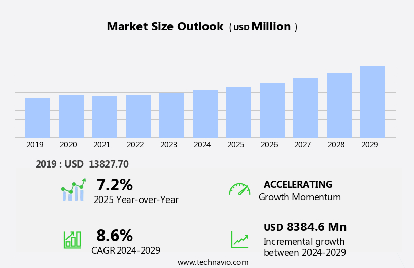
The semiconductor chemical vapor deposition equipment market size is forecast to increase by USD 8.38 billion at a CAGR of 8.6% between 2024 and 2029.
- The market is experiencing significant growth due to the increasing demand for advanced electronics in various industries, particularly in automotive electronics. companies in this market are responding to this trend by launching new CVD systems to cater to the growing demand. Cloud computing and machine learning have transformed the semiconductor industry, enabling data storage technology and connected devices to become smarter and more efficient. Additionally, alternative deposition techniques, such as plasma-enhanced CVD and atomic layer deposition, are gaining popularity due to their ability to produce high-quality films with improved uniformity and precision. These advancements are driving the growth of the market. Furthermore, the increasing miniaturization of electronic devices and the need for higher performance and reliability are also fueling the market's expansion.
What will be the Size of the Market During the Forecast Period?
- The market is experiencing significant growth due to the increasing demand for advanced semiconductor technologies. The integration of IoT devices in various industries, including telecommunications, biomedical, and industrial automation, is driving the need for next-generation semiconductors with superior electronic properties. Wafer fabrication processes have evolved, necessitating the use of advanced materials and green technology in semiconductor equipment. Materials science plays a crucial role in the development of high-performance materials for CVD processes, which contribute to cost reduction and yield improvement. The semiconductor shortage has highlighted the importance of process optimization and supply chain efficiency in the semiconductor industry.
- Furthermore, robotics and automation have become essential in semiconductor manufacturing, ensuring precision engineering and cleanroom technology are maintained to the highest standards. The future of electronics lies in nanotechnology, quantum computing, and 5G technology. These technologies require advanced CVD equipment capable of depositing thin films with exceptional optical and magnetic properties. Semiconductor research and development are focused on next-generation semiconductors, including silicon carbide and other high-performance materials, to meet the demands of these emerging technologies. The integration of these technologies in semiconductor equipment has led to significant advancements in the field, including the development of smart devices and renewable energy applications.
How is this market segmented and which is the largest segment?
The market research report provides comprehensive data (region-wise segment analysis), with forecasts and estimates in "USD million" for the period 2025-2029, as well as historical data from 2019-2023 for the following segments.
- Type
- Plasma-enhanced CVD
- Low-pressure CVD
- Atmospheric pressure CVD
- Metal-organic CVD
- End-user
- Foundries
- Integrated device manufacturers (IDMs)
- Geography
- APAC
- China
- India
- Japan
- South Korea
- North America
- US
- Europe
- Germany
- UK
- France
- South America
- Brazil
- Middle East and Africa
- APAC
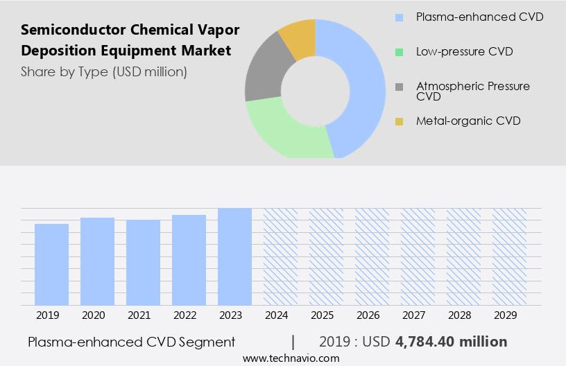
By Type Insights
- The plasma-enhanced CVD segment is estimated to witness significant growth during the forecast period.
The semiconductor chemical vapor deposition (CVD) equipment market encompasses various types of CVD processes, with Plasma-induced CVD (PECVD) being a significant segment. PECVD is a specialized CVD process that employs plasma to enhance reactivity in the gas phase, enabling the deposition of films at lower temperatures. This results in better control over film properties, making PECVD ideal for depositing dielectric layers, passivation films, and encapsulation coatings. These applications are essential in manufacturing Micro-Electro-Mechanical Systems (MEMS), Light light-emitting diodes (LEDs), and integrated circuits.
Furthermore, PECVD's ability to deposit high-quality dielectric layers is crucial for MEMS devices, which demand precise and reliable insulating layers. PECVD plays a vital role in producing advanced semiconductor components, including IoT devices and high-performance electric devices, as substitutes for traditional technologies.
Get a glance at the market report of share of various segments Request Free Sample
The plasma-enhanced CVD segment was valued at USD 4.78 billion in 2019 and showed a gradual increase during the forecast period.
Regional Analysis
- APAC is estimated to contribute 50% to the growth of the global market during the forecast period.
Technavio's analysts have elaborately explained the regional trends and drivers that shape the market during the forecast period.

For more insights on the market share of various regions Request Free Sample
The Asia-Pacific (APAC) region dominates the global semiconductor chemical vapor deposition (CVD) equipment market due to its significance as the primary location for semiconductor manufacturing. Key countries, such as China, South Korea, Japan, and Taiwan, are at the helm of the semiconductor industry. Major players in the region drive the demand for advanced CVD systems in this region. These nations contribute substantially to global semiconductor production, necessitating CVD equipment for manufacturing logic devices, memory chips, and other sophisticated semiconductor products. The semiconductor industry's advancements, particularly in high aspect ratio technologies and 3D packaging, fuel the need for CVD equipment in the production of advanced semiconductor devices for electronic devices and 5G networks.
Market Dynamics
Our researchers analyzed the data with 2024 as the base year, along with the key drivers, trends, and challenges. A holistic analysis of drivers will help companies refine their marketing strategies to gain a competitive advantage.
What are the key market drivers leading to the rise in adoption of Semiconductor Chemical Vapor Deposition Equipment Market?
Growth in automotive electronics is the key driver of the market.
- The market is experiencing substantial growth due to the increasing demand for advanced semiconductors in various industries. In particular, the expansion of the automotive sector, driven by the rise of electric vehicles (EVs), autonomous driving systems, and advanced driver-assistance systems (ADAS), is fueling this demand. In 2023, the global EV market witnessed a significant increase, with nearly 14 million new electric cars registered, bringing the total number of electric vehicles on the roads to 40 million. Semiconductors play a crucial role in these vehicles, enabling applications such as sensors, power management, and connectivity modules.
- Beyond the automotive sector, the semiconductor CVD equipment market is also being driven by the need for high-performance semiconductors in various electronic devices, including 5G networks, high-performance computing (HPC), IoT devices, wearables, and medical devices. These devices require thin films and high-purity solid materials for their manufacturing, which can be achieved through CVD processes. Moreover, the increasing urbanization and the resulting demand for energy-efficient solutions, as well as the emergence of new materials such as graphene, are creating new opportunities for the semiconductor CVD equipment market. The market is also being driven by the development of new precursor delivery mechanisms, such as atomic layer deposition (ALD) and plasma-enhanced CVD (PECVD), which offer improved deposition conditions and reach.
What are the market trends shaping the Semiconductor Chemical Vapor Deposition Equipment Market?
New product launches by companies is the upcoming trend in the market.
- The market is experiencing substantial growth due to the increasing demand for advanced semiconductors and electronic devices. This market is driven by the need for high aspect ratio structures, 3D packaging, and the integration of new materials such as graphene, thin films, and high-purity solid materials in semiconductor manufacturing. The emergence of 5G networks, IoT, autonomous vehicles, infotainment systems, wireless communication systems, and wearables are also significant factors fueling the market's expansion. Semiconductor manufacturers and academia are focusing on developing energy-efficient processes and improving deposition conditions to enhance manufacturing capacity and reach new markets in urbanization and emerging economies.
- The market encompasses thermal chemical vapor deposition (TCVD) and plasma-enhanced CVD (PECVD) systems, as well as precursor delivery mechanisms such as AP CVD and PECVD. Key applications for semiconductor CVD equipment include the production of semiconductor devices, electronic devices, data storage devices, and various coatings for surface-related characteristics, such as metallic coatings for collision detection systems and catalytic coatings for medical devices and AI programs. The market is also witnessing innovation in high-performance, electric vehicles, and substitutes for traditional semiconductor components, such as IoT devices. The Environmental Protection Agency (EPA) plays a crucial role in regulating the semiconductor manufacturing industry, ensuring that CVD equipment adheres to environmental standards.
What challenges does Semiconductor Chemical Vapor Deposition Equipment Market face during its growth?
Alternative deposition techniques is a key challenge affecting the market growth.
- The market experiences competition from alternative deposition techniques, including atomic layer deposition (ALD) and physical vapor deposition (PVD), which can substitute CVD in specific applications. ALD's ability to deposit ultra-thin, uniform layers with atomic-scale thickness and achieve precise control over film thickness and composition makes it an attractive choice for advanced semiconductor manufacturing processes, such as those below 7 nm and 3D devices. This technique's high conformality and high-quality films are essential for emerging applications in areas like 5G networks, high-performance computing (HPC), urbanization, energy-efficient technologies, and IoT devices. Additionally, ALD's applicability extends to various industries, including electronics, medical devices, and wearables, where surface-related characteristics and catalytic coatings are crucial.
- The semiconductor industry's ongoing innovation and the increasing demand for energy-efficient and high-performance materials continue to drive the growth of both CVD and ALD markets. Semiconductor manufacturing capacity expansion, driven by the CHIPS Act and ICs demand, further boosts the market's potential. Precursor delivery mechanisms, such as AP CVD and plasma-enhanced CVD, also contribute to the market's reach and versatility. The market's supply chain continues to evolve, with environmental protection agency regulations playing a significant role in shaping the industry's future.
Exclusive Customer Landscape
The market forecasting report includes the adoption lifecycle of the market, covering from the innovator's stage to the laggard's stage. It focuses on adoption rates in different regions based on penetration. Furthermore, the market report also includes key purchase criteria and drivers of price sensitivity to help companies evaluate and develop their market growth analysis strategies.

Customer Landscape
Key Companies & Market Insights
Companies are implementing various strategies, such as strategic alliances, market forecast, partnerships, mergers and acquisitions, geographical expansion, and product/service launches, to enhance their presence in the market.
ADEKA Corp: The company offers semiconductor chemical vapor deposition systems that are utilized for a variety of applications such as film creation, surface chemistry, and functional polymers.
The market research and growth report includes detailed analyses of the competitive landscape of the market and information about key companies, including:
- AIXTRON SE
- Applied Materials Inc.
- ASM International NV
- CVD Equipment Corp.
- IBC Coatings Technologies Inc.
- KOKUSAI ELECTRIC CORP
- Lam Research Corp.
- Oxford Instruments plc
- PLASMA THERM
- PVD Products Inc.
- Semicore Equipment Inc.
- Sulzer Ltd.
- Tokyo Electron Ltd.
- Ulvac Inc.
- Veeco Instruments Inc.
Qualitative and quantitative analysis of companies has been conducted to help clients understand the wider business environment as well as the strengths and weaknesses of key market players. Data is qualitatively analyzed to categorize companies as pure play, category-focused, industry-focused, and diversified; it is quantitatively analyzed to categorize companies as dominant, leading, strong, tentative, and weak.
Research Analyst Overview
The market plays a pivotal role in the manufacturing process of advanced semiconductors, enabling the deposition of thin films with high precision and accuracy. This technology is essential in producing high aspect ratio structures, which are crucial for 3D packaging and the development of semiconductor devices for various applications. The semiconductor industry's relentless pursuit of innovation drives the demand for CVD equipment. The integration of CVD technology in semiconductor manufacturing is instrumental in creating high-performance semiconductors for electronic devices, such as smartphones, computers, and servers.
Furthermore, the emergence of new technologies, including 5G networks, High-Performance Computing (HPC), and the Internet of Things (IoT), necessitates the continuous development of semiconductors with improved surface-related characteristics, energy efficiency, and thermal stability. Academia and industries collaborate to explore new materials and deposition conditions for CVD equipment. For instance, researchers have been investigating the use of graphene and other new materials in semiconductor manufacturing. These materials offer unique properties, such as high electrical conductivity, thermal stability, and mechanical strength, making them attractive alternatives for semiconductor components. The semiconductor CVD equipment market is influenced by several factors, including the increasing demand for energy-efficient semiconductors in emerging markets, the growing need for high-purity solid materials in various industries, and the increasing manufacturing capacity to meet the demands of the semiconductor industry.
|
Market Scope |
|
|
Report Coverage |
Details |
|
Page number |
206 |
|
Base year |
2024 |
|
Historic period |
2019-2023 |
|
Forecast period |
2025-2029 |
|
Growth momentum & CAGR |
Accelerate at a CAGR of 8.6% |
|
Market Growth 2025-2029 |
USD 8.38 billion |
|
Market structure |
Fragmented |
|
YoY growth 2024-2025(%) |
7.2 |
|
Key countries |
US, China, Japan, Germany, UK, India, France, Brazil, South Korea, and Australia |
|
Competitive landscape |
Leading Companies, Market Positioning of Companies, Competitive Strategies, and Industry Risks |
What are the Key Data Covered in this Market Research and Growth Report?
- CAGR of the market during the forecast period
- Detailed information on factors that will drive the market growth and forecasting between 2025 and 2029
- Precise estimation of the size of the market and its contribution of the market in focus to the parent market
- Accurate predictions about upcoming market growth and trends and changes in consumer behaviour
- Growth of the market across APAC, North America, Europe, South America, and Middle East and Africa
- Thorough analysis of the market's competitive landscape and detailed information about companies
- Comprehensive analysis of factors that will challenge the growth of market companies
We can help! Our analysts can customize this market research report to meet your requirements. Get in touch
 RIA -
RIA - 
